সহযোগিতা
কলা
সৌন্দর্য এবং সুস্থতা
ক্রাফট
সংস্কৃতি ও ইতিহাস
বিনোদন
পরিবেশ
খাদ্য ও পানীয়
রিভার্স ইঞ্জিনিয়ারিং
বিজ্ঞান
খেলাধুলা
টেকনোলজি
পরিধানযোগ্য
অন-চিপ SRAM: একটি শ্বাস-প্রশ্বাসের আলো যা আপনার চিপের নিজস্ব মেমরিতে সংরক্ষিত
English
Youblob (simulation output) · CC0
Ed

তৈরি করেছেন

Ed

29. সেপ্টেম্বর 2026FI
৪৯
০
০
০
০

অন-চিপ SRAM: একটি শ্বাস-প্রশ্বাসের আলো যা আপনার চিপের নিজস্ব মেমরিতে সংরক্ষিত

wafer.space-এর টেমপ্লেটের উদাহরণ ডিজাইনে SRAM ম্যাক্রো রয়েছে দুটি, প্রতিটি ৫১২ বাইট, এবং সেগুলো বন্ধ অবস্থায় রাখা হয়েছে। ম্যাক্রো হলো PDK থেকে একটি তৈরি মেমরি ব্লক: ৪,০৯৬টি স্ট্যাটিক মেমরি সেল, যেগুলো একবারে ঠিকানা ডিকোডার ও রিড সার্কিটসহ আঁকা হয়েছে, এবং আপনি গেট দিয়ে তৈরি না করে সম্পূর্ণ একটি ব্লক হিসেবে বসান। এই ধাপে একটি চালু করা হয়। আগের ধাপের PWM ডিমার এখন একটি প্যাটার্ন চালায়: একটি মাইক্রোকন্ট্রোলার প্যাডের মাধ্যমে চিপে ২৫৬ বাইট একবার লেখে, এবং এরপর চিপ নিজে থেকেই প্রতি ধাপে একটি করে বাইট পড়ে, ধীরে শ্বাস নেওয়া আলোর উজ্জ্বলতা হিসেবে। এই ব্লুপ্রিন্টের জন্য কোর ও টেস্টবেঞ্চ Icarus Verilog 12.0, cocotb 2.1.0 এবং PDK-এর নিজস্ব SRAM ম্যাক্রোর সিমুলেশন মডেল দিয়ে চালানো হয়েছে: আউটপুট ৬০০টি PWM পিরিয়ড ধরে সংরক্ষিত টেবিল অনুসরণ করেছে। ছবিটি সেই সিমুলেশনের নিজস্ব আউটপুট, প্রতি পিরিয়ডে একটি বার। টেবিল লোড করা ESP32 স্কেচটি এই ব্লুপ্রিন্টের জন্য কম্পাইল করা হয়েছে; এটি চালানোর জন্য এখনো কোনো চিপ নেই।
উন্নত
একটি সন্ধ্যা, আর চিপ

নির্দেশাবলি

1

প্যাটার্ন, সময় এবং আকার

Jupyter নোটবুক লোড হচ্ছে…
2

৪,০৯৬টি বিটের প্রতিটি আসলে কী

এমবেডেড ব্লুপ্রিন্টটি দেখায় কীভাবে একটি স্ট্যাটিক মেমরি বিট নিজেকে ধরে রাখে: দুটি ইনভার্টারের একটি লুপ। এই ধাপের ম্যাক্রো হলো একটি অ্যারেতে ৪,০৯৬টি স্ট্যাটিক মেমরি বিট।
3

ম্যাক্রোর পিন, এবং এর মডেল যে তিনটি বিষয় বলে

gf180mcu_fd_ip_sram__sram512x8m8wm1 512 বাইট ধারণ করে। এর পিনগুলো: CLK; A, একটি 9-bit ঠিকানা; D, লেখার বাইট; Q, পড়া বাইট। তিনটি নিয়ন্ত্রণ সবই সক্রিয় LOW স্তরে থাকে। CEN ০ থাকলে মেমোরি চালু হয়। GWEN ০ থাকলে ক্লক এজ একটি লেখা হিসেবে গণ্য হয়, ১ থাকলে পড়া। WEN প্রতি ডেটা বিটের জন্য একটি বিট, এবং ০ হলে সেই বিটটি লেখা যায়, তাই একটি লেখার কাজে একটি বাইটের কিছু বিট বদলানো যায় এবং বাকিগুলো অপরিবর্তিত রাখা যায়। PDK-এর সিমুলেশন মডেল পড়লে তিনটি জানার মতো বিষয় পাওয়া যায়। প্রথমত, CEN ১ থেকে ০ হওয়ার পরেই মেমোরি কাজ করে; অন্যথায় মডেল "CEN is not reset, memory is not operational" বার্তা দেয়, তাই core রিসেটের সময় CEN ১ রাখে এবং পরে নামিয়ে দেয়। দ্বিতীয়ত, পড়ার সময় A নমুনা নেওয়া ক্লক এজের ঠিক পরে Q-তে mem[A] আসে, তাই ডেটা এক ক্লক পরে প্রস্তুত হয়। তৃতীয়ত, মডেল প্রতিটি বাইট ০ দিয়ে শুরু হয়। বাস্তব চিপ তা করে না: এর SRAM পাওয়ার-আপে প্রতিটি সেল যে অবস্থায় পড়েছিল তা ধরে রাখে, তাই ডিজাইনকে পড়ার আগে লিখতে হবে। টেমপ্লেটের নিজের উদাহরণে CEN ১-এ যুক্ত, তাই এর দুটি ম্যাক্রো বন্ধ অবস্থায় থাকে। এর টাইমিং ফাইলে ম্যাক্রোর ন্যূনতম ক্লক পিরিয়ড দেওয়া আছে: টাইপিক্যাল ৫ V কর্নারে ৬.৬ ns এবং ধীর ৩.০ V, ১২৫ °C কর্নারে ১৮.৩ ns, উভয়ই টেমপ্লেটের ৪০ ns-এর মধ্যে ভালোভাবে পড়ে।
4

The core

src/chip_core.sv for the pattern player, with the template's port list unchanged plus one parameter, HOLD_LOG2. Input pad 0 enables, pad 1 selects LOAD mode, pad 2 is the write strobe; bidirectional pads 0 to 7 carry the byte, pad 8 the PWM. The LOAD and strobe pads are passed through two flip-flops before use, a synchroniser: they change whenever the outside world likes, not in step with the chip's clock, and a flip-flop caught mid-change can hover between 0 and 1 for a while. In play mode, each time HOLD_LOG2 periods have passed, the byte the SRAM has been reading becomes the new duty and the address moves on.
chip_core.svsystemverilog
// SPDX-License-Identifier: Apache-2.0
// Youblob silicon rung 5: the PWM dimmer plays a brightness pattern stored in the on-chip SRAM macro.
// Port list unchanged from wafer-space/gf180mcu-project-template src/chip_core.sv.

`default_nettype none

module chip_core #(
    parameter NUM_INPUT_PADS,
    parameter NUM_BIDIR_PADS,
    parameter NUM_ANALOG_PADS,
    parameter HOLD_LOG2 = 9        // each table entry lasts 2**HOLD_LOG2 PWM periods
    )(
    `ifdef USE_POWER_PINS
    inout  wire VDD,
    inout  wire VSS,
    `endif

    input  wire clk,       // clock
    input  wire rst_n,     // reset (active low)

    input  wire [NUM_INPUT_PADS-1:0] input_in,   // Input value
    output wire [NUM_INPUT_PADS-1:0] input_pu,   // Pull-up
    output wire [NUM_INPUT_PADS-1:0] input_pd,   // Pull-down

    input  wire [NUM_BIDIR_PADS-1:0] bidir_in,   // Input value
    output wire [NUM_BIDIR_PADS-1:0] bidir_out,  // Output value
    output wire [NUM_BIDIR_PADS-1:0] bidir_oe,   // Output enable
    output wire [NUM_BIDIR_PADS-1:0] bidir_cs,   // Input type (0=CMOS Buffer, 1=Schmitt Trigger)
    output wire [NUM_BIDIR_PADS-1:0] bidir_sl,   // Slew rate (0=fast, 1=slow)
    output wire [NUM_BIDIR_PADS-1:0] bidir_ie,   // Input enable
    output wire [NUM_BIDIR_PADS-1:0] bidir_pu,   // Pull-up
    output wire [NUM_BIDIR_PADS-1:0] bidir_pd,   // Pull-down

    inout  wire [NUM_ANALOG_PADS-1:0] analog  // Analog
);

    // Input pad 0: enable.  Input pad 1: LOAD mode.  Input pad 2: write strobe.
    // Bidir pads 0..7: the byte to store while loading.  Bidir pad 8: the PWM output.
    localparam DUTY_W = 8;
    localparam PWM_PAD = 8;

    assign input_pu = '0;
    assign input_pd = '0;
    assign bidir_oe = {{(NUM_BIDIR_PADS-DUTY_W){1'b1}}, {DUTY_W{1'b0}}};
    assign bidir_ie = ~bidir_oe;
    assign bidir_cs = {{(NUM_BIDIR_PADS-DUTY_W){1'b0}}, {DUTY_W{1'b1}}};
    assign bidir_sl = '0;
    assign bidir_pu = '0;
    assign bidir_pd = '0;

    wire enable = input_in[0];
    wire [DUTY_W-1:0] data_in = bidir_in[DUTY_W-1:0];

    // The mode and strobe pads change whenever the outside world likes, not in step with clk:
    // two flip-flops in a row (a synchroniser) before anything uses them.
    logic [1:0] load_s;
    logic [2:0] strobe_s;
    always_ff @(posedge clk) begin
        load_s   <= {load_s[0], input_in[1]};
        strobe_s <= {strobe_s[1:0], input_in[2]};
    end
    logic load_was;
    wire load        = load_s[1];
    wire load_start  = load & ~load_was;
    wire strobe_rise = strobe_s[1] & ~strobe_s[2];
    always_ff @(posedge clk) load_was <= load;

    // The SRAM wants its chip enable (CEN, active LOW) to go 1 -> 0 before it works:
    // hold it at 1 through reset, then 0.
    logic cen;
    always_ff @(posedge clk) cen <= !rst_n;

    // PWM counter and the "hold" counter that decides when to step to the next table entry.
    logic [DUTY_W-1:0] count;
    logic [HOLD_LOG2:0] hold;                   // one bit wider so HOLD_LOG2 = 0 still works
    wire period_end = (count == '1);
    localparam logic [HOLD_LOG2:0] HOLD_MASK = (1 << HOLD_LOG2) - 1;   // 0 when HOLD_LOG2 = 0
    wire step = period_end && ((hold & HOLD_MASK) == HOLD_MASK);

    logic [DUTY_W-1:0] addr;
    logic [DUTY_W-1:0] duty;
    wire  [DUTY_W-1:0] q;                       // SRAM read data: mem[addr], one clock after addr

    always_ff @(posedge clk) begin
        if (!rst_n) begin
            count <= '0;  hold <= '0;  addr <= '0;  duty <= '0;
        end else if (load) begin
            count <= '0;  hold <= '0;  duty <= '0;
            if (load_start)       addr <= '0;       // every load starts at entry 0
            else if (strobe_rise) addr <= addr + 1'b1;
        end else if (enable) begin
            count <= count + 1'b1;
            if (period_end) hold <= hold + 1'b1;
            if (step) begin
                duty <= q;                          // the entry that was being read
                addr <= addr + 1'b1;                // and move on to the next
            end
        end
    end

    `gf180mcu_xxx_ip_sram__sram512x8m8wm1 sram_0 (
        `ifdef USE_POWER_PINS
        .VDD  (VDD),
        .VSS  (VSS),
        `endif
        .CLK  (clk),
        .CEN  (cen),                                   // active low: 0 = on
        .GWEN (~(load && strobe_rise)),                // active low: 0 = write this clock
        .WEN  (8'b0),                                  // active low, per bit: write all eight
        .A    ({1'b0, addr}),                          // 256 of the 512 bytes
        .D    (data_in),
        .Q    (q)
    );

    logic pwm;
    always_ff @(posedge clk) begin
        if (!rst_n) pwm <= 1'b0;
        else        pwm <= enable && !load && (count < duty);
    end

    logic [NUM_BIDIR_PADS-1:0] out;
    always_comb begin
        out = '0;
        out[PWM_PAD] = pwm;
    end
    assign bidir_out = out;

    // Inputs this design does not read (keeps lint quiet, as the template does with _unused).
    logic _unused;
    assign _unused = &{1'b0, input_in[NUM_INPUT_PADS-1:3], bidir_in[NUM_BIDIR_PADS-1:DUTY_W], hold[HOLD_LOG2]};

endmodule

`default_nettype wire

প্রয়োজনীয় সরঞ্জাম:

ডেস্কটপ কম্পিউটারডেস্কটপ কম্পিউটার
5

The test

test_pattern.py builds the core with the PDK's SRAM model, gf180mcu_fd_ip_sram__sram512x8m8wm1.v, at the template's 25 MHz and with HOLD_LOG2 = 0 so the whole table plays in 256 periods. It loads the table through the pads the way the ESP32 will, then counts the high clocks in each of 600 PWM periods and requires them to follow the table from exactly one starting point. A second test loads again and checks the new pattern replaced the old.
test_pattern.pypython
# SPDX-License-Identifier: Apache-2.0
# cocotb testbench for the SRAM pattern player, with the PDK's own SRAM simulation model
# (gf180mcu_fd_ip_sram__sram512x8m8wm1, gf180mcuD, the commit the template pins).
import math
import os
from pathlib import Path

import cocotb
from cocotb.clock import Clock
from cocotb.triggers import ClockCycles, FallingEdge, RisingEdge
from cocotb_tools.runner import get_runner

PWM_PAD = 8
EN, LOAD, STROBE = 1, 2, 4                      # input pad bits
SRAM = Path(os.getenv("PDK_ROOT", "pdk")) / "gf180mcuD" / "libs.ref" / "gf180mcu_fd_ip_sram" / "verilog"


def breathing_table(n=256, gamma=2.2):
    """One slow breath: a raised sine, gamma-corrected so equal steps LOOK equal to the eye."""
    return [round(255 * ((1 - math.cos(2 * math.pi * i / n)) / 2) ** gamma) for i in range(n)]


async def start(dut):
    cocotb.start_soon(Clock(dut.clk, 40, unit="ns").start())   # 25 MHz, the template's CLOCK_PERIOD
    dut.input_in.value = 0
    dut.bidir_in.value = 0
    dut.rst_n.value = 0
    await ClockCycles(dut.clk, 5)
    dut.rst_n.value = 1
    await ClockCycles(dut.clk, 2)


async def load(dut, table):
    """What a microcontroller on the breakout does: LOAD high, then per byte set the data pads,
    raise the strobe, wait, lower it. The chip synchronises the strobe, so hold each for 4 clocks."""
    dut.input_in.value = LOAD
    await ClockCycles(dut.clk, 4)
    for b in table:
        dut.bidir_in.value = b
        await ClockCycles(dut.clk, 1)
        dut.input_in.value = LOAD | STROBE
        await ClockCycles(dut.clk, 4)
        dut.input_in.value = LOAD
        await ClockCycles(dut.clk, 4)
    dut.input_in.value = 0
    await ClockCycles(dut.clk, 4)


async def highs_per_period(dut, periods):
    """High clocks in each PWM period, counted from the core's own count = 0."""
    while int(dut.count.value) != 0:
        await RisingEdge(dut.clk)
    out = []
    for _ in range(periods):
        n = 0
        for _ in range(256):
            await FallingEdge(dut.clk)
            n += int(dut.bidir_out.value[PWM_PAD])
        out.append(n)
    return out


@cocotb.test()
async def test_plays_the_table(dut):
    """Load a 256-entry breathing table, play it: each period's high time is the next entry."""
    table = breathing_table()
    await start(dut)
    await load(dut, table)
    dut.input_in.value = EN
    got = await highs_per_period(dut, 600)
    # the output starts part-way through the table; find where, then demand every period match
    fits = [off for off in range(256) if all(got[j] == table[(j + off) % 256] for j in range(2, 600))]
    dut._log.info(f"first periods {got[:8]}, table aligns at offset {fits}")
    Path(__file__).resolve().parent.joinpath("pattern_trace.csv").write_text("\n".join(map(str, got)))
    assert len(fits) == 1, f"the output does not follow the table (offsets that fit: {fits})"


@cocotb.test()
async def test_reload(dut):
    """Loading again replaces the pattern: a flat 64 gives 64 high clocks every period."""
    await start(dut)
    await load(dut, breathing_table())
    await load(dut, [64] * 256)
    dut.input_in.value = EN
    got = await highs_per_period(dut, 40)
    assert all(g == 64 for g in got[2:]), got


def test_runner():
    here = Path(__file__).resolve().parent
    defines = {"gf180mcu_xxx_ip_sram__sram512x8m8wm1": "gf180mcu_fd_ip_sram__sram512x8m8wm1"}
    runner = get_runner("icarus")
    runner.build(
        sources=[SRAM / "gf180mcu_fd_ip_sram__sram512x8m8wm1.v", here / "chip_core.sv"],
        hdl_toplevel="chip_core",
        parameters={"NUM_INPUT_PADS": 4, "NUM_BIDIR_PADS": 38, "NUM_ANALOG_PADS": 4, "HOLD_LOG2": 0},
        defines=defines,
        build_args=["-g2012"],
        timescale=("1ns", "1ps"),
        always=True,
    )
    runner.test(hdl_toplevel="chip_core", test_module="test_pattern")


if __name__ == "__main__":
    test_runner()

প্রয়োজনীয় সরঞ্জাম:

ডেস্কটপ কম্পিউটারডেস্কটপ কম্পিউটার
6

simulation-এর মুদ্রিত ফলাফল

এই blueprint-এর জন্য Icarus Verilog 12.0 এবং cocotb 2.1.0 দিয়ে চালানো হয়েছে: -------- MESSAGE: CEN এইমাত্র reset হয়েছে, memory কার্যকর আছে --------- test_pattern.test_plays_the_table PASS (600 periods, table ঠিক একটি offset-এ align হয়) test_pattern.test_reload PASS TESTS=2 PASS=2 FAIL=0 SKIP=0 টেস্ট ব্যর্থ হতে পারে তা প্রমাণ করতে, WEN-এর মান 8'b0 থেকে 8'hFF-এ পরিবর্তন করা হয়েছিল, active-low pin-এর ক্লাসিক ভুল: প্রতিটি bit masked, কিছুই লেখা হয়নি, একটি শূন্যের table। দুটি টেস্টই ব্যর্থ হয়েছে, এবং core আবার আগের অবস্থায় ফিরিয়ে আনা হয়েছে। প্রথম লাইনটি SRAM model-এর নিজস্ব বার্তা: reset-এর পর model-এর প্রয়োজন অনুযায়ী core CEN নামিয়েছে।
7

Load it from an ESP32

Once the chip is on its breakout board, this sketch writes the table. Eight GPIOs carry the byte, three more drive LOAD, the strobe and enable, and an LED with a 330 ohm resistor from pad 8 to ground shows the breath. Each level is held for 1 microsecond, 25 of the chip's clocks, so the synchroniser always sees it. The sketch then does nothing: the pattern lives in the chip. It is lost when the chip loses power, so send r over serial to load it again. The ESP32 is a 3.3 V part and its inputs are not 5 V tolerant. The sketch only drives the chip and never reads from it. The template's default libraries are the 5 V ones; before you connect, check in the I/O library's documentation that 3.3 V is a valid logic high for your chip's inputs, or build with the 3.3 V libraries, as the template's README shows. The sketch compiles for the ESP32 with the Arduino ESP32 core 3.3.12; it has not been run, because the chip does not exist yet.
load_pattern.inocpp
// SPDX-License-Identifier: Apache-2.0
// Load a breathing pattern into your chip's SRAM through its pads, then let the chip play it.
// Youblob silicon rung 5. The chip does the playing; this board only writes 256 bytes once.
//
// Wiring (ESP32 GPIO -> chip pad on your breakout):
//   D0..D7  GPIO 13,14,18,19,21,22,23,25 -> bidir[0..7]
//   LOAD    GPIO 26 -> input[1]
//   STROBE  GPIO 27 -> input[2]
//   EN      GPIO 32 -> input[0]
//   and a common ground. The chip's bidir[8] drives an LED through 330 ohm to ground.
// The ESP32 is a 3.3 V part: run the chip's I/O at 3.3 V, or put a level shifter between them.

#include <math.h>

const int DATA_PINS[8] = {13, 14, 18, 19, 21, 22, 23, 25};
const int PIN_LOAD = 26, PIN_STROBE = 27, PIN_EN = 32;

// The chip passes LOAD and STROBE through a two-flip-flop synchroniser and looks for the strobe's
// rising edge, so every level has to last a few of ITS clocks. 1 us is 25 clocks at 25 MHz.
const unsigned HOLD_US = 1;

uint8_t table[256];

void makeBreathingTable() {
  // a raised sine, gamma-corrected (2.2) so the brightness steps look even to the eye
  for (int i = 0; i < 256; i++) {
    float s = (1.0f - cosf(2.0f * PI * i / 256.0f)) / 2.0f;
    table[i] = (uint8_t)lroundf(255.0f * powf(s, 2.2f));
  }
}

void putByte(uint8_t b) {
  for (int bit = 0; bit < 8; bit++) digitalWrite(DATA_PINS[bit], (b >> bit) & 1);
  delayMicroseconds(HOLD_US);            // data settles before the strobe
  digitalWrite(PIN_STROBE, HIGH);        // the chip writes on the strobe's rising edge...
  delayMicroseconds(HOLD_US);            // ...a few of its clocks later, so hold the data
  digitalWrite(PIN_STROBE, LOW);
  delayMicroseconds(HOLD_US);
}

void loadTable() {
  digitalWrite(PIN_EN, LOW);
  digitalWrite(PIN_LOAD, HIGH);          // entering LOAD resets the chip's address to 0
  delayMicroseconds(HOLD_US);
  for (int i = 0; i < 256; i++) putByte(table[i]);
  digitalWrite(PIN_LOAD, LOW);
  delayMicroseconds(HOLD_US);
}

void setup() {
  Serial.begin(115200);
  for (int bit = 0; bit < 8; bit++) pinMode(DATA_PINS[bit], OUTPUT);
  pinMode(PIN_LOAD, OUTPUT);
  pinMode(PIN_STROBE, OUTPUT);
  pinMode(PIN_EN, OUTPUT);
  digitalWrite(PIN_STROBE, LOW);

  makeBreathingTable();
  loadTable();
  digitalWrite(PIN_EN, HIGH);            // play
  Serial.println("pattern loaded; the chip is playing it on its own");
  Serial.printf("table[0]=%u table[64]=%u table[128]=%u\n", table[0], table[64], table[128]);
}

void loop() {
  // Nothing to do: the pattern lives in the chip's SRAM now.
  // Send 'r' over serial to load it again (the SRAM loses it when the chip loses power).
  if (Serial.available() && Serial.read() == 'r') {
    loadTable();
    digitalWrite(PIN_EN, HIGH);
    Serial.println("reloaded");
  }
}

এই ধাপের উপকরণ:

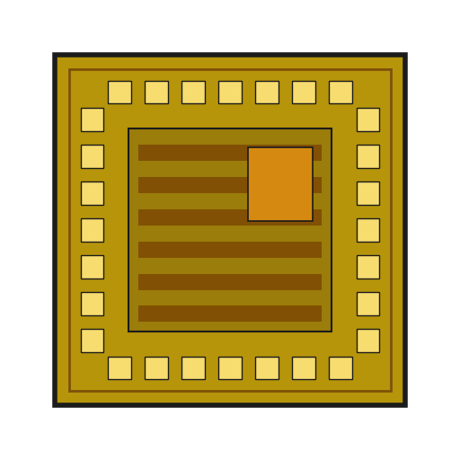
কাস্টম ASIC ডাইকাস্টম ASIC ডাই1 টুকরা
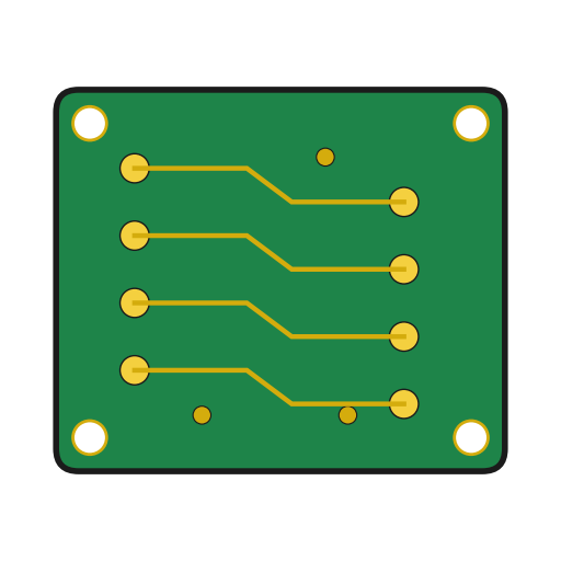
মুদ্রিত বর্তনী বোর্ডমুদ্রিত বর্তনী বোর্ড1 টুকরা
৫ মিমির এলইডি৫ মিমির এলইডি1 টুকরা
৩৩০ ওহম রোধক৩৩০ ওহম রোধক1 টুকরা

প্রয়োজনীয় সরঞ্জাম:

ESP32 উন্নয়ন বোর্ডESP32 উন্নয়ন বোর্ড
ব্রেডবোর্ডব্রেডবোর্ড
জাম্পার তারজাম্পার তার
ডেস্কটপ কম্পিউটারডেস্কটপ কম্পিউটার
8

একটি প্যাটার্ন যা সংরক্ষণ হচ্ছে না বা চলছে না

SRAM প্যাটার্নের সমস্যা সমাধান।

Flow

Loading...
9

Sources and honest limits

**Sources**, 29 सेप्टेंबर 2026-এ পড়া হয়েছে: GF180MCU PDK টেমপ্লেট যে কমিটে পিন করে সেখানে (gf180mcuD, f6eeac7dad085ffcc829ccfd721f7b4ce39edcf7, fossi-foundation ciel রিলিজ থেকে; Apache-2.0): SRAM মডেল gf180mcu_fd_ip_sram__sram512x8m8wm1.v, এর outline-এর জন্য LEF এবং ন্যূনতম clock period-এর জন্য এর timing ফাইলসমূহ; flip-flop এলাকার জন্য standard-cell লাইব্রেরির timing ফাইল। wafer-space/gf180mcu-project-template রিপোজিটরি (src/chip_core.sv, src/chip_top.sv, README.md, librelane/config.yaml; Apache-2.0). **Honest limits.** সিমুলেশনটি chip_core লেভেলে, SRAM-এর নিজস্ব মডেল ব্যবহার করে কিন্তু pad ring, synthesis বা layout ছাড়া; এখানে মডেলের timing checks কিছুই নির্ধারণ করে না। ESP32 স্কেচটি কম্পাইল করা হয়েছিল, চালানো হয়নি। পরীক্ষায় HOLD_LOG2 ছিল 0 যাতে এটি শেষ হয়; চিপে এটি 9 হতো, প্রায় 1.3 s-এর একটি বিরতি।

উপকরণ

4

প্রয়োজনীয় সরঞ্জাম

4

CC0 পাবলিক ডোমেন

এই ব্লুপ্রিন্ট CC0-এর অধীনে প্রকাশিত। আপনি অনুমতি ছাড়াই যেকোনো উদ্দেশ্যে এটি অনুলিপি, পরিবর্তন, বিতরণ ও ব্যবহার করতে পারেন।

মেকারের ব্লুপ্রিন্টের মাধ্যমে পণ্য কিনে তাঁকে সমর্থন করুন, যেখানে তিনি আয় করেন মেকার কমিশন বিক্রেতাদের নির্ধারিত, অথবা এই ব্লুপ্রিন্টের একটি নতুন সংস্করণ তৈরি করে নিজের ব্লুপ্রিন্টে সংযোগ হিসেবে যুক্ত করে আয় ভাগ করুন।

আলোচনা

(0)

লগ ইন করুন আলোচনায় যোগ দিতে

মন্তব্য লোড হচ্ছে...