སྒྱུ་རྩལ
མཛེས་སྡུག་དང་བདེ་ཐང
བཟོ་རིག
རིག་གནས་དང་ལོ་རྒྱུས
དགའ་སྟོན
ཁོར་ཡུག
ཟས་དང་བཏུང་རྫས
ཕྱིར་འཕྲུལ་རིག
ཚན་རིག
རྩེད་འགྲན
རིག་རྩལ
གྱོན་རུང
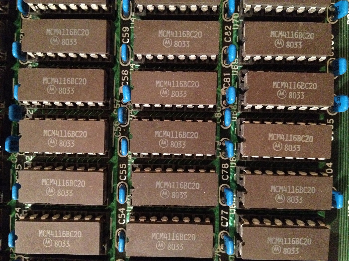

The DRAM Cell
Robert Dennard's cell, patented at IBM in 1968 from a 1966 idea, is the most-manufactured object in human history. More DRAM cells exist than grains of sand on most beaches, and each one is a transistor and a capacitor and nothing else.
The idea is almost insultingly simple. To store a bit, put charge on a capacitor. To keep it private, put a switch in front of the capacitor and leave the switch open. To read or write, close the switch.
One transistor, one capacitor. Compare it with what came before, in the two blueprints this one links back to: magnetic core memory needed a ferrite ring threaded by hand with three or four wires, and a mercury delay line needed a tube of mercury and a transducer at each end. Compare it with the alternative that arrived alongside it — static RAM, the sibling blueprint — which needs six transistors per bit. Dennard's cell is the smallest way anyone has found to store a bit in silicon, and smallest means cheapest, and cheapest is why it won.
The price is in the word DYNAMIC. Nothing holds the charge on that capacitor. It leaks — through the access transistor which is never perfectly off, through the junction into the substrate, through the dielectric. A cell written as a 1 becomes an unreadable 0 in something between milliseconds and a second.
So the memory must read every cell and write it back before the charge falls too far, continuously, forever. That is refresh, and it is not a design flaw bolted on afterwards. It is the direct and unavoidable consequence of storing information as charge on an isolated node, and every DRAM ever made has spent part of its life doing it instead of serving the processor.
You will build a single cell from a discrete MOSFET and a capacitor, watch a stored bit die on a scope, measure its half-life, and then measure how much shorter that half-life gets when you warm it up.
མཐོ་རིམ
6 hours
ལམ་སྟོན
1
1
The cell, drawn
The cell, drawn
Two components. Look at the schematic and note what is NOT there: no feedback, no latch, no power connection to the storage node at all. Once the wordline goes low, that node is connected to nothing, and the only thing keeping the bit alive is the charge sitting on the capacitor's plates.
That isolation is the whole design. It is why the cell is small, and it is why the bit dies.
THE ACCESS TRANSISTOR is an ordinary n-channel MOSFET. Its gate is the wordline, shared by every cell in a row. Its drain goes to the bitline, shared by every cell in a column. Its source is the storage node. So a cell is addressed by raising one wordline and reading one bitline, and the array is a grid — which is the second reason DRAM is cheap: the wiring per cell is two wires shared with thousands of neighbours.
THE CAPACITOR is the part that got hard. In a modern cell it holds around 25 femtofarads, and it has to hold that in a footprint of a few hundred square nanometres. A flat plate of that capacitance would be enormous, so the industry went vertical: trench capacitors etched down into the substrate with aspect ratios past 50:1, or stacked capacitors built up above it. Getting 25 fF into that area is genuinely one of the hardest things done in manufacturing, and it is why DRAM is made by a handful of companies.
Your bench version will use a 100 pF capacitor, which is four thousand times larger. That makes the retention time convenient to measure rather than impossibly short, and the physics is unchanged.
KiCanvas བལྟ་མི་ཐོབ་བཞིན...
ཆེད་ལས PCB བཀོད་པ་བལྟ་མི
ལག་ཆས་དགོས་མཁོ:
 ཅོག་ཙེའི་གློག་རིག
2
2
Build it and watch a bit die
Build it and watch a bit die
Two components on a breadboard, and one measurement that has to be done carefully or it measures your instrument instead of the cell.
THE BUILD. A 2N7000 n-channel MOSFET. Gate to a pin you can drive — that is the wordline. Drain to another driven pin through 1 kilohm — that is the bitline. Source to one leg of a 100 pF ceramic capacitor, other leg to ground. The junction of source and capacitor is the storage node.
THE PROBLEM WITH MEASURING IT, and this is the step people get wrong. A scope probe is 1 megohm or 10 megohms to ground. Put that on a node holding charge on 100 pF and the RC time constant is 100 microseconds or 1 millisecond — so the probe drains the cell far faster than leakage does, and you measure your probe.
You must either use a 10x probe with 10 megohm input and accept that you are measuring probe plus cell, or buffer the node. Buffering is better: a JFET-input op-amp as a unity-gain follower has an input impedance in the gigohms and will not load the node measurably. Build the follower, connect its input to the storage node and its output to the scope.
State plainly which you did, because the retention figure means nothing without it.
NOW WRITE A BIT. Set the bitline pin high, pulse the wordline high for a few milliseconds, then bring the wordline low. The capacitor is charged and isolated. Set the bitline pin to input so it floats and cannot hold the node up through the transistor's leakage.
WATCH IT ON THE SCOPE, DC coupled, slow timebase — 1 second per division to start. You will see the stored voltage decay: fast at first if your transistor leaks, then slower. Photograph the trace.
MEASURE THE RETENTION TIME. Define a threshold, say 60 percent of the written voltage, below which the bit can no longer be read reliably as a 1. Time from the write to that crossing. That is your retention time and it is the number the whole architecture is built around.
EXPECT VARIATION BETWEEN PARTS. Try five transistors. Retention will vary by a factor of several, because leakage is dominated by whichever imperfection happens to be worst in that device. Real DRAM has exactly this problem at a scale of billions: the refresh interval is set by the WORST cell on the chip, not the average, and a handful of unusually leaky cells force the entire array to be refreshed far more often than it needs. Chips ship with redundant rows specifically to replace them.
གོམ་པ་འདིའི་རྫས་རིགས:
 N ལམ་གྱི་MOSFET (2N7000)10 དུམ་བུ།
 རྫ་མཁན་གྱི་ཀོན་ཌེན་སར་ཆ་ཚན།1 ཚན་པ།
 JFET ཨོཔ་ཨེམཔ། (TL071)5 དུམ་བུ།
 འགོག་ཆས་ཀྱི་ཚོགས་ཆས།1 ཚན་པ།
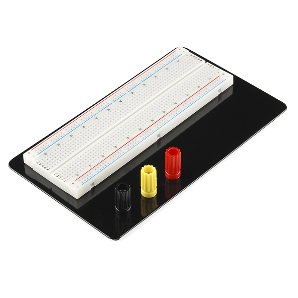 Breadboard1 དུམ་བུ།
 མཐུད་ཐག་ཆ་ཚན།1 ཚན་པ།
ལག་ཆས་དགོས་མཁོ:
 ཨོ་སི་ལོ་སི་ཀོབ།
 ཞིབ་དཔྱད་ཁང་ཚད་གཞི་ཅན་གྱི་ཨང་རྟགས་སྣ་མང་འཇལ་ཆས།
 ཅོག་ཙེའི་གློག་མཁོ་སྤྲོད།
 ཆུ་ཚོད་བཀག་ཆས།
3
3
Log retention against temperature
Log retention against temperature
A scope trace gives you one number. What you want is a distribution, and how it moves with temperature — because temperature is what actually sets the refresh interval in a real part.
This sketch writes a 1 into the cell, then samples the storage node repeatedly until the bit is no longer readable, logging voltage against time as CSV. It repeats five times and reads a DS18B20 so every run is stamped with the cell temperature.
ONE THING IN THE SKETCH IS WORTH READING CAREFULLY, because it is not a workaround, it is how real DRAM behaves. Reading the cell requires opening the access transistor, which connects the storage capacitor to the bitline and to the ADC input. Charge is shared, so the act of reading DISTURBS the bit. In a real DRAM this is worse than a disturbance — the read is destructive, and the sense amplifier must immediately write the value back into the cell it just read. That write-back is not an optimisation, it is a requirement, and it is why a DRAM read cycle is longer than you would expect from the array alone.
Here the sketch simply re-writes and starts a new run. Note in your results that the sampled decay curve is slightly faster than the true leakage, because every sample takes a little charge. Sampling less often gives a truer curve and worse resolution, which is a real measurement trade rather than a defect.
RUN IT AT TWO TEMPERATURES. Room temperature first, then warm the transistor with a hairdryer to 50 or 60 degrees and run again. Junction leakage roughly doubles every 8 to 10 degrees Celsius, so expect retention to fall by a factor of four or more over that range.
That is why server DRAM refreshes twice as often above 85 degrees, and why memory in a hot rack costs more bandwidth to maintain than the same memory in a cool one.
dram_logger.inocpp
གོམ་པ་འདིའི་རྫས་རིགས:
 ESP32 གོང་འཕེལ་པང་ལེབ།1 དུམ་བུ།
 DS18B20 དྲོད་ཚད་ཚོར་ཆས།1 དུམ་བུ།N ལམ་གྱི་MOSFET (2N7000)5 དུམ་བུ།རྫ་མཁན་གྱི་ཀོན་ཌེན་སར་ཆ་ཚན།1 ཚན་པ།Breadboard1 དུམ་བུ།
ལག་ཆས་དགོས་མཁོ:
 ཞ་སྦྱོར་གྱི་ལས་སྡེ།ཞིབ་དཔྱད་ཁང་ཚད་གཞི་ཅན་གྱི་ཨང་རྟགས་སྣ་མང་འཇལ་ཆས།ཅོག་ཙེའི་གློག་རིག
 ཞིབ་དཔྱད་ཁང་གི་ཚ་གྲང་འཇལ་ཆས།
4
4
Refresh — what it costs to keep the bits alive
Refresh — what it costs to keep the bits alive
Jupyter ཚང་དེབ་མངོན་གསལ་འབད་དོ་…
ལག་ཆས་དགོས་མཁོ:
ཅོག་ཙེའི་གློག་རིག5
5
What DRAM replaced
What DRAM replaced
Before you leave this cell, look at what it displaced, because the comparison is the reason DRAM matters rather than merely works.
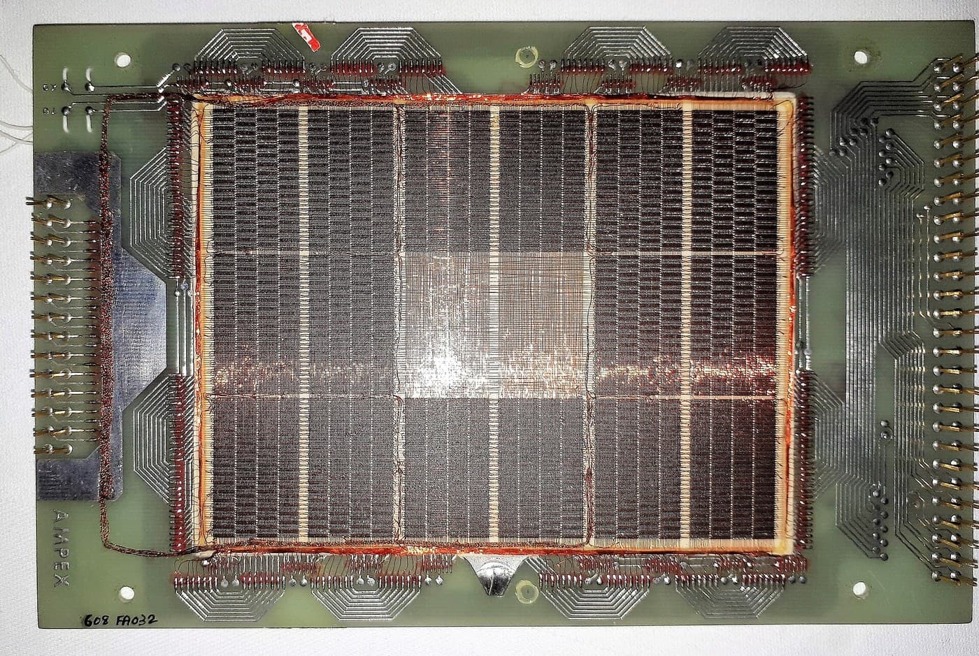
Magnetic core memory is embedded below rather than referenced, because it is worth actually reading. Every bit is a ferrite ring with wires threaded through it BY HAND — through the 1960s, largely by women working with needles and magnifiers, at a cost per bit that no amount of process improvement was ever going to fix. Core is non-volatile, which DRAM is not, and it survived a total power loss, which is why Apollo flew it.
Dennard's cell beat it on one axis only: it can be PRINTED. Photolithography defines a million cells in the same exposure as one, so the cost per bit falls with every process generation instead of tracking the price of skilled labour.
That is the same argument the Noyce blueprint makes about interconnect, arriving in a different place. Printed beats placed, not because the printed thing is better, but because its cost does not scale with quantity.
Core memory's non-volatility, incidentally, is a genuine advantage that took the industry fifty years to get back. The floating gate in the next-but-one blueprint is the answer, and it arrived in 1971 — one year after the Intel 1103 made DRAM commercial.
རྫས་རིགས
8- 15 དུམ་བུ།ས་ཆ་འཛིན
- 1 ཚན་པ།ས་ཆ་འཛིན
- 5 དུམ་བུ།ས་ཆ་འཛིན
- ས་ཆ་འཛིན
- Breadboard - Classicཁེ་ཕོགས 10%1 དུམ་བུ།$9.46
- 1 ཚན་པ།ས་ཆ་འཛིན
- 1 དུམ་བུ།ས་ཆ་འཛིན
- 1 དུམ་བུ།ས་ཆ་འཛིན
ལག་ཆས་དགོས་མཁོ
7- ས་ཆ་འཛིན
- ས་ཆ་འཛིན
- ས་ཆ་འཛིན
- ས་ཆ་འཛིན
- ས་ཆ་འཛིན
- ས་ཆ་འཛིན
ཚོད་དཔག་བསྡོམས
བཟོ་མི་གིས་ཉོ་མི་དེ། གོང་ཚད་མེད་པར་སྟོན་མི་ཅ་ཆས་ཚུ་ཁྱོད་ཀྱིས་ག་ཏེ་ལས་ཉོཝ་ཨིན་ན་དེ་ལས་ཐོབ་ཨིན།
འབྲེལ་ཡོད་བིལུ་པིརིན་ཊི
བིལུ་པིརིན་ཊི་འདི་ཚུ་ཐབས་ལམ་དང་རྫས་རིགས། སྤྱི་ཆོས་བགོ་བཤའ་བྱེད

CC0 སྤྱི་དབང
བིལུ་པིརིན་ཊི་འདི་CC0 འོག་བཀྲམས་ཡོད། ཁྱེད་རང་གིས་ཆོག་མཆན་མ་བཞེས་པར་ཕབ་ལེན་དང་བཟོ་བཅོས། བགོ་བཤའ། དགོས་མཁོ་གང་ལའང་བཀོལ་སྤྱོད་བྱས་ཆོག
བཟོ་མཁན་ལ་རྒྱབ་སྐྱོར་བྱེད་པའི་ཆེད་ཁོང་ཚོའི་བིལུ་པིརིན་ཊི་བརྒྱུད་ཐོན་སྐྱེད་ཉོ། བཟོ་མཁན་གྱིས བཟོ་མཁན་གྱི་ཁེ་ཕོགས ཚོང་པས་གཏན་འཁེལ་བྱས་པ། ཡང་ན་བིལུ་པིརིན་ཊི་འདིའི་པར་གསར་བཟོས་ཏེ་ཁྱེད་རང་གི་བིལུ་པིརིན་ཊི་ནང་མཐུད་སྦྲེལ་བྱས་ཏེ་ཡོང་སྒོ་བགོ་བཤའ་བྱེད།