艺术
美容与健康
工艺
文化与历史
娱乐
环境
食品与饮料
逆向工程
科学
体育
技术
可穿戴设备

The Semiconductor Laser Diode
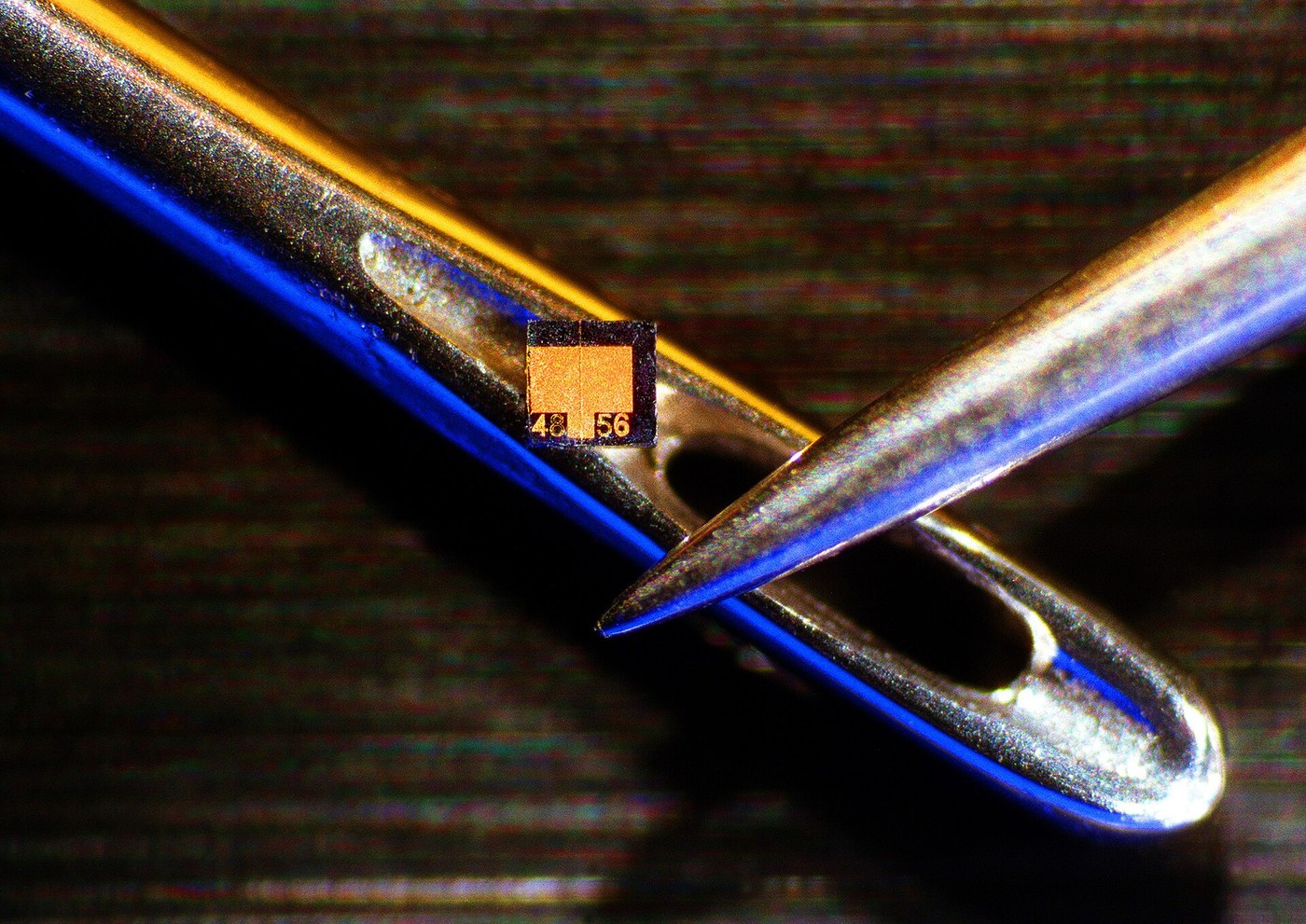
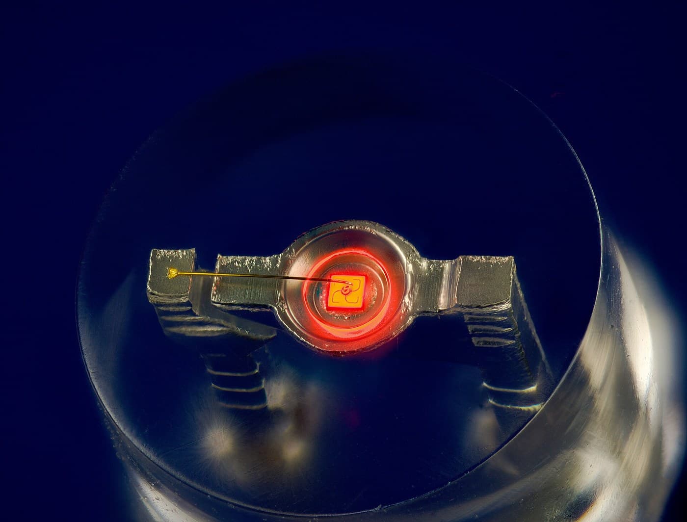
In the autumn of 1962 four groups reported a laser made from a piece of gallium arsenide the size of a grain of salt: Robert Hall at General Electric Schenectady, Marshall Nathan at IBM, Nick Holonyak at GE Syracuse with the first visible one, and Quist and Rediker at MIT Lincoln Laboratory. All of them worked only in pulses, and only when dunked in liquid nitrogen.
The reason is that a plain GaAs junction confines nothing. Injected carriers wander off before they recombine, and the light spreads out of the thin active region into absorbing material. The threshold current density was tens of thousands of amps per square centimetre, which a chip can only survive for a microsecond at a time.
The fix took eight years and arrived twice at once in 1970: Zhores Alferov's group at the Ioffe Institute and Izuo Hayashi and Morton Panish at Bell Labs both made the DOUBLE HETEROSTRUCTURE work. Sandwich a thin layer of GaAs between two layers of AlGaAs, which has a wider bandgap AND a lower refractive index, and you get both confinements from one sandwich: the carriers cannot climb out, and the light is trapped in a waveguide. Threshold fell by a factor of about a hundred and the diode ran continuously at room temperature. Alferov and Herbert Kroemer shared the 2000 Nobel Prize for it.
FULLY BUILDABLE. This blueprint is the sibling of the LED blueprint, and the difference between them is measurable in an afternoon: build a proper current-source driver, sweep the current, and find the knee where the same junction stops being an LED and starts being a laser. The driver is the real skill here, because the commonest way a maker destroys a laser diode is by driving it from a voltage source.
中级
5 hours
说明
1
1
Start from the LED
Start from the LED
Build or re-read the LED blueprint first. A laser diode is the same forward-biased junction, injecting electrons and holes into the same active layer, recombining across the same bandgap. Everything about the colour is identical.
Two things are added, and only two. A CAVITY: the crystal is cleaved along a lattice plane, and the refractive index step from about 3.5 to 1.0 at the cleaved face reflects roughly 30 % without any coating at all. Two parallel cleaved faces are a Fabry-Perot cavity that costs nothing to make. And ENOUGH CURRENT to invert the junction, so stimulated emission outruns spontaneous.
Keep the LED on the bench. You will sweep both and compare the curves.
所需工具:
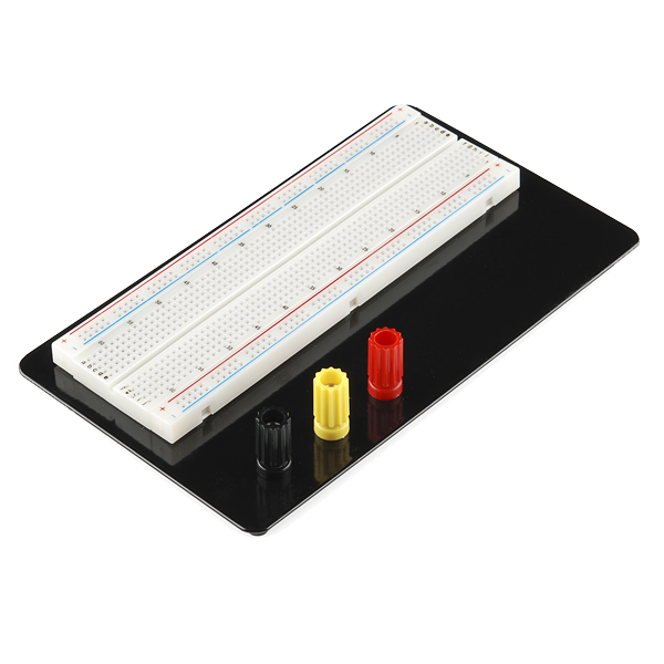 Breadboard - Classic
 跳线套装
跳线套装 电阻套件
电阻套件 实验室级数字万用表
2
2
Build the constant-current driver
Build the constant-current driver
Build the driver on the breadboard. The op-amp holds the voltage across R_SENSE equal to the command voltage, so the diode current is V_SET divided by 10 ohms and nothing the diode does can change it. Use an LM358, not a TL071: on a single 5 V supply the LM358's inputs work down to 0 V, and this circuit commands 0 to 0.59 V. R1 (75k) over the 10k pot caps the command at 0.59 V, about 58 mA.
Three details are not optional. R_SS and C_SS ramp the command with a time constant of about a second, because a laser diode is killed by a switch-on SPIKE far more often than by a steady overcurrent. D_PROT clamps reverse voltage, because the reverse breakdown of a laser diode is only a few volts. C_COMP with R_F damps the loop so a change of setting does not overshoot into the diode.
Checked in ngspice: the current follows V_SET / 10 ohms to within 0.4 % (the transistor's base current) from 0 to 60 mA; switched on at full setting it rises smoothly to 58 mA, 63 % at 1.1 s and 99 % at 5.5 s, with no spike; a 10 mA step overshoots by about 0.9 mA without C_COMP and not at all with it. The simulation used a behavioural LM358-class op-amp and generic transistor and diode models, not vendor models, so it proves the circuit's behaviour, not your parts' exact figures.
Before connecting the diode, test the loop with an ordinary red LED in its place and verify with the multimeter that the current follows the pot and holds steady when you warm the LED with your fingers.
加载 KiCanvas 查看器...
专业 PCB 设计查看器
此步骤所需材料:
 运算放大器集成电路1 个
 NPN 晶体管1 个
 阻断二极管(肖特基)1 个
 LED 套件1 个运算放大器集成电路1 个NPN 晶体管1 个阻断二极管(肖特基)1 个LED 套件1 个电阻套件1 个
 电容套件1 个
 10 千欧线性电位器1 个
所需工具:
Breadboard - Classic跳线套装实验室级数字万用表 台式电源
台式电源3
3
Sweep the current and log the light
Sweep the current and log the light
Wire GPIO25 to the driver's command input in place of the pot wiper, and the monitor photodiode through R_MON to GPIO34. Set I_MAX_MA below your diode's absolute maximum from its datasheet before you flash anything.
Wear the goggles and point the diode into a matte card. Open the serial monitor at 115200 and capture the CSV.
The sketch starts dark, measures the dark level, steps up in forty points with a 5 s settle at each, about three and a half minutes in all, and finishes dark. The settle matters twice: the slow-start filter needs five time constants to reach each new setting (at 40 ms the current has moved only a few percent of the way), and read too fast you would also catch the junction warming up rather than the L-I curve. The sketch reports the current the DAC actually commands, in steps of about 1.3 mA, not the value it asked for.
laser_diode_li_sweep.inocpp
此步骤所需材料:
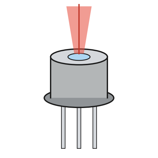 激光二极管1 个
 光电二极管(BPW34)1 个电阻套件1 个
所需工具:
 ESP32 开发板Breadboard - Classic跳线套装
 激光防护镜
激光防护镜 台式电脑实验室级数字万用表
4
4
Find the knee, the slope and the temperature coefficient
Find the knee, the slope and the temperature coefficient
正在加载 Jupyter 笔记本…
所需工具:
台式电脑5
5
Compendium: from liquid nitrogen to the fibre link
Compendium: from liquid nitrogen to the fibre link
WHY 1962 NEEDED LIQUID NITROGEN. A homojunction confines neither carriers nor light. Injected electrons diffuse a micrometre or more before recombining and the optical mode spills into absorbing material either side, so threshold current density ran to tens of thousands of amps per square centimetre at room temperature — survivable only in microsecond pulses at 77 K.
WHAT THE DOUBLE HETEROSTRUCTURE CHANGED. AlGaAs has both a wider bandgap and a lower refractive index than GaAs, so a thin GaAs layer between two AlGaAs layers is simultaneously a potential well for carriers and a dielectric waveguide for photons. Both confinements from one sandwich, and threshold current density fell to the low hundreds of amps per square centimetre. Alferov at the Ioffe Institute, and Hayashi and Panish at Bell Labs, reached room-temperature continuous operation independently in 1970.
THE FACETS ARE THE CAVITY. The chip is cleaved along a crystal plane, giving two mirrors flat to atomic dimensions and parallel by construction, with about 30 % reflectivity uncoated from the index step of 3.5 to 1.0. Put L = 300 micrometres into the Fabry-Perot blueprint's free spectral range and the modes come out about 140 GHz apart — which is why a bare Fabry-Perot diode emits a comb of lines rather than one, and why telecom lasers add a distributed Bragg grating to pick a single mode.
SIBLING TABLE AGAINST THE LED. LED: no cavity, spontaneous emission only, 20 to 40 nm wide, Lambertian, no threshold, tolerant of any old supply and a series resistor. Laser diode: cleaved-facet cavity, stimulated emission above threshold, about 1 nm wide, a beam roughly 10 by 30 degrees, a sharp threshold, and an absolute requirement for a current source. Below threshold the laser diode IS an LED, and you measured the changeover in step 4.
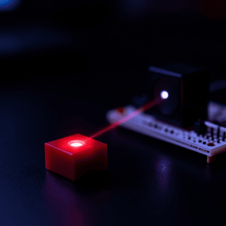
WHERE THIS LEADS. The laser-communicator blueprint in the catalogue modulates a laser module with audio; that module is this blueprint's subject. Everything after this in the batch assumes a source like it — small, cheap, directly modulated at gigahertz rates by varying its current, and working at 1310 or 1550 nm instead of red.
材料
9- 1 个占位符
- 2 个占位符
- 2 个占位符
- 2 个占位符
- 占位符
- 1 个占位符
- 1 个占位符
- 1 个占位符
- 1 个占位符
相关蓝图
这些蓝图共享知识——技术、材料或原理


CC0 公共领域
此蓝图以 CC0 协议发布。你可以自由复制、修改、分发和使用此作品,无需征得许可。
通过购买蓝图中的产品支持创客,他们将获得 创客佣金 (由供应商设定),或创建此蓝图的新版本并将其作为连接包含在你自己的蓝图中以分享收入。