Zusammenarbeit
KUNST
SCHÖNHEIT & WELLNESS
HANDWERK
KULTUR & GESCHICHTE
UNTERHALTUNG
UMFELD
ESSEN & GETRÄNKE
REVERSE ENGINEERING
WISSENSCHAFTEN
SPORT
TECHNOLOGIE
WEARABLES
Der On-Chip-SRAM: Ein atmendes Licht, gespeichert im eigenen Speicher des Chips
English
Youblob (simulation output) · CC0
Ed

Erstellt von

Ed

29. September 2026FI
51
0
0
0
0

Der On-Chip-SRAM: Ein atmendes Licht, gespeichert im eigenen Speicher des Chips

Die Vorlage von wafer.space enthält in ihrem Beispieldesign zwei SRAM-Makros mit je 512 Byte und lässt sie ausgeschaltet. Ein Makro ist ein fertiger Speicherblock aus dem PDK: 4.096 statische Speicherzellen, einmal mit ihrem Adressdecoder und ihren Leseschaltungen entworfen, die man als Ganzes platziert, statt sie aus Gattern aufzubauen. Diese Stufe schaltet einen davon ein. Der PWM-Dimmer aus der vorherigen Stufe spielt nun ein Muster ab: Ein Mikrocontroller schreibt einmalig 256 Byte über die Pads in den Chip, und danach liest der Chip sie selbstständig Byte für Byte, Schritt für Schritt, als Helligkeit eines langsam atmenden Lichts zurück. Der Kern und sein Testbench wurden für diese Blaupause mit Icarus Verilog 12.0, cocotb 2.1.0 und dem eigenen Simulationsmodell des PDK für das SRAM-Makro ausgeführt: Der Ausgang folgte der gespeicherten Tabelle über 600 PWM-Perioden. Das Bild ist die eigene Ausgabe dieser Simulation, ein Balken pro Periode. Die ESP32-Skizze, die die Tabelle lädt, wurde für diese Blaupause kompiliert; es gibt noch keinen Chip, auf dem sie laufen könnte.
Erfahren
Ein Abend, plus der Chip

Anweisungen

1

Das Muster, das Timing und die Größe

Jupyter-Notebook wird geladen …
2

Was jedes der 4.096 Bits ist

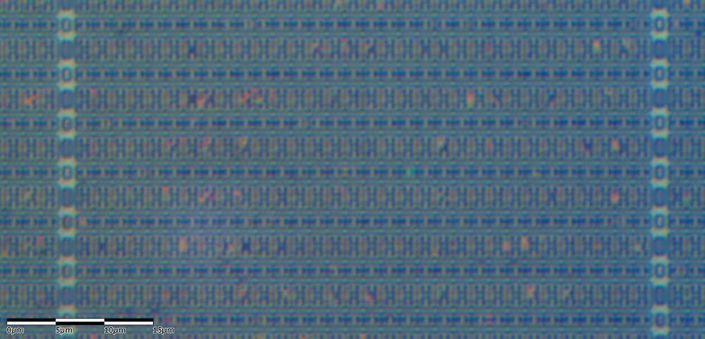
Der eingebettete Bauplan zeigt, wie ein Bit statischen Speichers sich selbst hält: eine Schleife aus zwei Invertern. Das Makro in dieser Stufe besteht aus 4.096 Bits statischen Speichers in einem Array.
3

Die Pins des Makros und drei Dinge, die sein Modell aussagt

gf180mcu_fd_ip_sram__sram512x8m8wm1 speichert 512 Bytes. Seine Pins: CLK; A, eine 9-Bit-Adresse; D, das zu schreibende Byte; Q, das gelesene Byte. Die drei Steuersignale sind alle aktiv LOW. CEN bei 0 schaltet den Speicher ein. GWEN bei 0 macht die Taktflanke zu einem Schreibvorgang, bei 1 zu einem Lesevorgang. WEN hat ein Bit pro Datenbit, und eine 0 erlaubt das Schreiben dieses Bits, sodass ein Schreibvorgang einige Bits eines Bytes ändern und die anderen unverändert lassen kann. Das Simulationsmodell des PDK zeigt drei wissenswerte Punkte. Erstens funktioniert der Speicher erst, nachdem CEN von 1 auf 0 gewechselt hat; das Modell gibt andernfalls "CEN is not reset, memory is not operational" aus, daher hält der Kern CEN während des Resets auf 1 und senkt es danach ab. Zweitens liefert ein Lesevorgang mem[A] kurz nach der Taktflanke, die A abgetastet hat, auf Q, sodass die Daten einen Takt später bereitstehen. Drittens startet das Modell mit jedem Byte auf 0. Ein echter Chip tut das nicht: sein SRAM startet in dem Zustand, den jede Zelle beim Einschalten zufällig annimmt, daher muss das Design schreiben, bevor es liest. Das Beispiel der Vorlage setzt CEN auf 1, sodass seine beiden Makros abgeschaltet sind. Seine Timing-Dateien geben die minimale Taktperiode des Makros mit 6,6 ns im typischen 5-V-Eckfall und 18,3 ns im langsamen 3,0-V-, 125-°C-Eckfall an, beide deutlich innerhalb der 40 ns der Vorlage.
4

The core

src/chip_core.sv for the pattern player, with the template's port list unchanged plus one parameter, HOLD_LOG2. Input pad 0 enables, pad 1 selects LOAD mode, pad 2 is the write strobe; bidirectional pads 0 to 7 carry the byte, pad 8 the PWM. The LOAD and strobe pads are passed through two flip-flops before use, a synchroniser: they change whenever the outside world likes, not in step with the chip's clock, and a flip-flop caught mid-change can hover between 0 and 1 for a while. In play mode, each time HOLD_LOG2 periods have passed, the byte the SRAM has been reading becomes the new duty and the address moves on.
chip_core.svsystemverilog
// SPDX-License-Identifier: Apache-2.0
// Youblob silicon rung 5: the PWM dimmer plays a brightness pattern stored in the on-chip SRAM macro.
// Port list unchanged from wafer-space/gf180mcu-project-template src/chip_core.sv.

`default_nettype none

module chip_core #(
    parameter NUM_INPUT_PADS,
    parameter NUM_BIDIR_PADS,
    parameter NUM_ANALOG_PADS,
    parameter HOLD_LOG2 = 9        // each table entry lasts 2**HOLD_LOG2 PWM periods
    )(
    `ifdef USE_POWER_PINS
    inout  wire VDD,
    inout  wire VSS,
    `endif

    input  wire clk,       // clock
    input  wire rst_n,     // reset (active low)

    input  wire [NUM_INPUT_PADS-1:0] input_in,   // Input value
    output wire [NUM_INPUT_PADS-1:0] input_pu,   // Pull-up
    output wire [NUM_INPUT_PADS-1:0] input_pd,   // Pull-down

    input  wire [NUM_BIDIR_PADS-1:0] bidir_in,   // Input value
    output wire [NUM_BIDIR_PADS-1:0] bidir_out,  // Output value
    output wire [NUM_BIDIR_PADS-1:0] bidir_oe,   // Output enable
    output wire [NUM_BIDIR_PADS-1:0] bidir_cs,   // Input type (0=CMOS Buffer, 1=Schmitt Trigger)
    output wire [NUM_BIDIR_PADS-1:0] bidir_sl,   // Slew rate (0=fast, 1=slow)
    output wire [NUM_BIDIR_PADS-1:0] bidir_ie,   // Input enable
    output wire [NUM_BIDIR_PADS-1:0] bidir_pu,   // Pull-up
    output wire [NUM_BIDIR_PADS-1:0] bidir_pd,   // Pull-down

    inout  wire [NUM_ANALOG_PADS-1:0] analog  // Analog
);

    // Input pad 0: enable.  Input pad 1: LOAD mode.  Input pad 2: write strobe.
    // Bidir pads 0..7: the byte to store while loading.  Bidir pad 8: the PWM output.
    localparam DUTY_W = 8;
    localparam PWM_PAD = 8;

    assign input_pu = '0;
    assign input_pd = '0;
    assign bidir_oe = {{(NUM_BIDIR_PADS-DUTY_W){1'b1}}, {DUTY_W{1'b0}}};
    assign bidir_ie = ~bidir_oe;
    assign bidir_cs = {{(NUM_BIDIR_PADS-DUTY_W){1'b0}}, {DUTY_W{1'b1}}};
    assign bidir_sl = '0;
    assign bidir_pu = '0;
    assign bidir_pd = '0;

    wire enable = input_in[0];
    wire [DUTY_W-1:0] data_in = bidir_in[DUTY_W-1:0];

    // The mode and strobe pads change whenever the outside world likes, not in step with clk:
    // two flip-flops in a row (a synchroniser) before anything uses them.
    logic [1:0] load_s;
    logic [2:0] strobe_s;
    always_ff @(posedge clk) begin
        load_s   <= {load_s[0], input_in[1]};
        strobe_s <= {strobe_s[1:0], input_in[2]};
    end
    logic load_was;
    wire load        = load_s[1];
    wire load_start  = load & ~load_was;
    wire strobe_rise = strobe_s[1] & ~strobe_s[2];
    always_ff @(posedge clk) load_was <= load;

    // The SRAM wants its chip enable (CEN, active LOW) to go 1 -> 0 before it works:
    // hold it at 1 through reset, then 0.
    logic cen;
    always_ff @(posedge clk) cen <= !rst_n;

    // PWM counter and the "hold" counter that decides when to step to the next table entry.
    logic [DUTY_W-1:0] count;
    logic [HOLD_LOG2:0] hold;                   // one bit wider so HOLD_LOG2 = 0 still works
    wire period_end = (count == '1);
    localparam logic [HOLD_LOG2:0] HOLD_MASK = (1 << HOLD_LOG2) - 1;   // 0 when HOLD_LOG2 = 0
    wire step = period_end && ((hold & HOLD_MASK) == HOLD_MASK);

    logic [DUTY_W-1:0] addr;
    logic [DUTY_W-1:0] duty;
    wire  [DUTY_W-1:0] q;                       // SRAM read data: mem[addr], one clock after addr

    always_ff @(posedge clk) begin
        if (!rst_n) begin
            count <= '0;  hold <= '0;  addr <= '0;  duty <= '0;
        end else if (load) begin
            count <= '0;  hold <= '0;  duty <= '0;
            if (load_start)       addr <= '0;       // every load starts at entry 0
            else if (strobe_rise) addr <= addr + 1'b1;
        end else if (enable) begin
            count <= count + 1'b1;
            if (period_end) hold <= hold + 1'b1;
            if (step) begin
                duty <= q;                          // the entry that was being read
                addr <= addr + 1'b1;                // and move on to the next
            end
        end
    end

    `gf180mcu_xxx_ip_sram__sram512x8m8wm1 sram_0 (
        `ifdef USE_POWER_PINS
        .VDD  (VDD),
        .VSS  (VSS),
        `endif
        .CLK  (clk),
        .CEN  (cen),                                   // active low: 0 = on
        .GWEN (~(load && strobe_rise)),                // active low: 0 = write this clock
        .WEN  (8'b0),                                  // active low, per bit: write all eight
        .A    ({1'b0, addr}),                          // 256 of the 512 bytes
        .D    (data_in),
        .Q    (q)
    );

    logic pwm;
    always_ff @(posedge clk) begin
        if (!rst_n) pwm <= 1'b0;
        else        pwm <= enable && !load && (count < duty);
    end

    logic [NUM_BIDIR_PADS-1:0] out;
    always_comb begin
        out = '0;
        out[PWM_PAD] = pwm;
    end
    assign bidir_out = out;

    // Inputs this design does not read (keeps lint quiet, as the template does with _unused).
    logic _unused;
    assign _unused = &{1'b0, input_in[NUM_INPUT_PADS-1:3], bidir_in[NUM_BIDIR_PADS-1:DUTY_W], hold[HOLD_LOG2]};

endmodule

`default_nettype wire

Benötigte Werkzeuge:

Desktop-ComputerDesktop-Computer
5

The test

test_pattern.py builds the core with the PDK's SRAM model, gf180mcu_fd_ip_sram__sram512x8m8wm1.v, at the template's 25 MHz and with HOLD_LOG2 = 0 so the whole table plays in 256 periods. It loads the table through the pads the way the ESP32 will, then counts the high clocks in each of 600 PWM periods and requires them to follow the table from exactly one starting point. A second test loads again and checks the new pattern replaced the old.
test_pattern.pypython
# SPDX-License-Identifier: Apache-2.0
# cocotb testbench for the SRAM pattern player, with the PDK's own SRAM simulation model
# (gf180mcu_fd_ip_sram__sram512x8m8wm1, gf180mcuD, the commit the template pins).
import math
import os
from pathlib import Path

import cocotb
from cocotb.clock import Clock
from cocotb.triggers import ClockCycles, FallingEdge, RisingEdge
from cocotb_tools.runner import get_runner

PWM_PAD = 8
EN, LOAD, STROBE = 1, 2, 4                      # input pad bits
SRAM = Path(os.getenv("PDK_ROOT", "pdk")) / "gf180mcuD" / "libs.ref" / "gf180mcu_fd_ip_sram" / "verilog"


def breathing_table(n=256, gamma=2.2):
    """One slow breath: a raised sine, gamma-corrected so equal steps LOOK equal to the eye."""
    return [round(255 * ((1 - math.cos(2 * math.pi * i / n)) / 2) ** gamma) for i in range(n)]


async def start(dut):
    cocotb.start_soon(Clock(dut.clk, 40, unit="ns").start())   # 25 MHz, the template's CLOCK_PERIOD
    dut.input_in.value = 0
    dut.bidir_in.value = 0
    dut.rst_n.value = 0
    await ClockCycles(dut.clk, 5)
    dut.rst_n.value = 1
    await ClockCycles(dut.clk, 2)


async def load(dut, table):
    """What a microcontroller on the breakout does: LOAD high, then per byte set the data pads,
    raise the strobe, wait, lower it. The chip synchronises the strobe, so hold each for 4 clocks."""
    dut.input_in.value = LOAD
    await ClockCycles(dut.clk, 4)
    for b in table:
        dut.bidir_in.value = b
        await ClockCycles(dut.clk, 1)
        dut.input_in.value = LOAD | STROBE
        await ClockCycles(dut.clk, 4)
        dut.input_in.value = LOAD
        await ClockCycles(dut.clk, 4)
    dut.input_in.value = 0
    await ClockCycles(dut.clk, 4)


async def highs_per_period(dut, periods):
    """High clocks in each PWM period, counted from the core's own count = 0."""
    while int(dut.count.value) != 0:
        await RisingEdge(dut.clk)
    out = []
    for _ in range(periods):
        n = 0
        for _ in range(256):
            await FallingEdge(dut.clk)
            n += int(dut.bidir_out.value[PWM_PAD])
        out.append(n)
    return out


@cocotb.test()
async def test_plays_the_table(dut):
    """Load a 256-entry breathing table, play it: each period's high time is the next entry."""
    table = breathing_table()
    await start(dut)
    await load(dut, table)
    dut.input_in.value = EN
    got = await highs_per_period(dut, 600)
    # the output starts part-way through the table; find where, then demand every period match
    fits = [off for off in range(256) if all(got[j] == table[(j + off) % 256] for j in range(2, 600))]
    dut._log.info(f"first periods {got[:8]}, table aligns at offset {fits}")
    Path(__file__).resolve().parent.joinpath("pattern_trace.csv").write_text("\n".join(map(str, got)))
    assert len(fits) == 1, f"the output does not follow the table (offsets that fit: {fits})"


@cocotb.test()
async def test_reload(dut):
    """Loading again replaces the pattern: a flat 64 gives 64 high clocks every period."""
    await start(dut)
    await load(dut, breathing_table())
    await load(dut, [64] * 256)
    dut.input_in.value = EN
    got = await highs_per_period(dut, 40)
    assert all(g == 64 for g in got[2:]), got


def test_runner():
    here = Path(__file__).resolve().parent
    defines = {"gf180mcu_xxx_ip_sram__sram512x8m8wm1": "gf180mcu_fd_ip_sram__sram512x8m8wm1"}
    runner = get_runner("icarus")
    runner.build(
        sources=[SRAM / "gf180mcu_fd_ip_sram__sram512x8m8wm1.v", here / "chip_core.sv"],
        hdl_toplevel="chip_core",
        parameters={"NUM_INPUT_PADS": 4, "NUM_BIDIR_PADS": 38, "NUM_ANALOG_PADS": 4, "HOLD_LOG2": 0},
        defines=defines,
        build_args=["-g2012"],
        timescale=("1ns", "1ps"),
        always=True,
    )
    runner.test(hdl_toplevel="chip_core", test_module="test_pattern")


if __name__ == "__main__":
    test_runner()

Benötigte Werkzeuge:

Desktop-ComputerDesktop-Computer
6

Was die Simulation ausgegeben hat

Lauf für diesen Blueprint mit Icarus Verilog 12.0 und cocotb 2.1.0: -------- MESSAGE: CEN ist gerade zurückgesetzt, Speicher ist betriebsbereit --------- test_pattern.test_plays_the_table PASS (600 Perioden, Tabelle passt an genau einem Offset) test_pattern.test_reload PASS TESTS=2 PASS=2 FAIL=0 SKIP=0 Um zu beweisen, dass der Test fehlschlagen kann, wurde WEN von 8'b0 auf 8'hFF geändert, der klassische Fehler mit einem active-low-Pin: jedes Bit maskiert, nichts geschrieben, eine Tabelle aus Nullen. Beide Tests schlugen fehl, und der Kern wurde wiederhergestellt. Die erste Zeile ist die eigene Meldung des SRAM-Modells: Der Kern hat CEN nach dem Reset heruntergezogen, wie es das Modell verlangt.
7

Load it from an ESP32

Once the chip is on its breakout board, this sketch writes the table. Eight GPIOs carry the byte, three more drive LOAD, the strobe and enable, and an LED with a 330 ohm resistor from pad 8 to ground shows the breath. Each level is held for 1 microsecond, 25 of the chip's clocks, so the synchroniser always sees it. The sketch then does nothing: the pattern lives in the chip. It is lost when the chip loses power, so send r over serial to load it again. The ESP32 is a 3.3 V part and its inputs are not 5 V tolerant. The sketch only drives the chip and never reads from it. The template's default libraries are the 5 V ones; before you connect, check in the I/O library's documentation that 3.3 V is a valid logic high for your chip's inputs, or build with the 3.3 V libraries, as the template's README shows. The sketch compiles for the ESP32 with the Arduino ESP32 core 3.3.12; it has not been run, because the chip does not exist yet.
load_pattern.inocpp
// SPDX-License-Identifier: Apache-2.0
// Load a breathing pattern into your chip's SRAM through its pads, then let the chip play it.
// Youblob silicon rung 5. The chip does the playing; this board only writes 256 bytes once.
//
// Wiring (ESP32 GPIO -> chip pad on your breakout):
//   D0..D7  GPIO 13,14,18,19,21,22,23,25 -> bidir[0..7]
//   LOAD    GPIO 26 -> input[1]
//   STROBE  GPIO 27 -> input[2]
//   EN      GPIO 32 -> input[0]
//   and a common ground. The chip's bidir[8] drives an LED through 330 ohm to ground.
// The ESP32 is a 3.3 V part: run the chip's I/O at 3.3 V, or put a level shifter between them.

#include <math.h>

const int DATA_PINS[8] = {13, 14, 18, 19, 21, 22, 23, 25};
const int PIN_LOAD = 26, PIN_STROBE = 27, PIN_EN = 32;

// The chip passes LOAD and STROBE through a two-flip-flop synchroniser and looks for the strobe's
// rising edge, so every level has to last a few of ITS clocks. 1 us is 25 clocks at 25 MHz.
const unsigned HOLD_US = 1;

uint8_t table[256];

void makeBreathingTable() {
  // a raised sine, gamma-corrected (2.2) so the brightness steps look even to the eye
  for (int i = 0; i < 256; i++) {
    float s = (1.0f - cosf(2.0f * PI * i / 256.0f)) / 2.0f;
    table[i] = (uint8_t)lroundf(255.0f * powf(s, 2.2f));
  }
}

void putByte(uint8_t b) {
  for (int bit = 0; bit < 8; bit++) digitalWrite(DATA_PINS[bit], (b >> bit) & 1);
  delayMicroseconds(HOLD_US);            // data settles before the strobe
  digitalWrite(PIN_STROBE, HIGH);        // the chip writes on the strobe's rising edge...
  delayMicroseconds(HOLD_US);            // ...a few of its clocks later, so hold the data
  digitalWrite(PIN_STROBE, LOW);
  delayMicroseconds(HOLD_US);
}

void loadTable() {
  digitalWrite(PIN_EN, LOW);
  digitalWrite(PIN_LOAD, HIGH);          // entering LOAD resets the chip's address to 0
  delayMicroseconds(HOLD_US);
  for (int i = 0; i < 256; i++) putByte(table[i]);
  digitalWrite(PIN_LOAD, LOW);
  delayMicroseconds(HOLD_US);
}

void setup() {
  Serial.begin(115200);
  for (int bit = 0; bit < 8; bit++) pinMode(DATA_PINS[bit], OUTPUT);
  pinMode(PIN_LOAD, OUTPUT);
  pinMode(PIN_STROBE, OUTPUT);
  pinMode(PIN_EN, OUTPUT);
  digitalWrite(PIN_STROBE, LOW);

  makeBreathingTable();
  loadTable();
  digitalWrite(PIN_EN, HIGH);            // play
  Serial.println("pattern loaded; the chip is playing it on its own");
  Serial.printf("table[0]=%u table[64]=%u table[128]=%u\n", table[0], table[64], table[128]);
}

void loop() {
  // Nothing to do: the pattern lives in the chip's SRAM now.
  // Send 'r' over serial to load it again (the SRAM loses it when the chip loses power).
  if (Serial.available() && Serial.read() == 'r') {
    loadTable();
    digitalWrite(PIN_EN, HIGH);
    Serial.println("reloaded");
  }
}

Materialien für diesen Schritt:

Eigener ASIC-DieEigener ASIC-Die1 Stück
LeiterplatteLeiterplatte1 Stück
5-mm-LED5-mm-LED1 Stück
330-Ohm-Widerstand330-Ohm-Widerstand1 Stück

Benötigte Werkzeuge:

ESP32-EntwicklungsboardESP32-Entwicklungsboard
SteckbrettSteckbrett
SteckbrückenSteckbrücken
Desktop-ComputerDesktop-Computer
8

Ein Muster, das nicht gespeichert wird oder nicht abgespielt werden kann

Fehlerbehebung bei SRAM-Mustern.

Flow

Loading...
9

Quellen und ehrliche Grenzen

**Quellen**, abgerufen am 29. September 2026: die GF180MCU PDK beim Commit, den die Vorlage festlegt (gf180mcuD, f6eeac7dad085ffcc829ccfd721f7b4ce39edcf7, aus den fossi-foundation-ciel-Releases; Apache-2.0): das SRAM-Modell gf180mcu_fd_ip_sram__sram512x8m8wm1.v, dessen LEF für den Umriss und dessen Timing-Dateien für die minimale Taktperiode; die Timing-Datei der Standardzellbibliothek für die Fläche des Flip-Flops. Das Repository wafer-space/gf180mcu-project-template (src/chip_core.sv, src/chip_top.sv, README.md, librelane/config.yaml; Apache-2.0). **Ehrliche Grenzen.** Die Simulation erfolgt auf der Ebene chip_core, mit dem eigenen Modell des SRAM, jedoch ohne Pad-Ring, Synthese oder Layout, und die Timing-Prüfungen des Modells entscheiden hier nichts. Die Skizze ESP32 wurde kompiliert, aber nicht ausgeführt. HOLD_LOG2 war im Test 0, damit sie terminiert; der Chip würde 9 verwenden, ein Atemzug von etwa 1,3 s.

Materialien

4

Benötigte Werkzeuge

4

CC0 Gemeinfrei

Dieser Blueprint ist unter CC0 veröffentlicht. Sie dürfen dieses Werk für jeden Zweck frei kopieren, ändern, verbreiten und verwenden, ohne um Erlaubnis zu fragen.

Unterstützen Sie den Maker, indem Sie Produkte über seinen Blueprint kaufen, wo er eine Maker-Provision von Anbietern festgelegt, verdient. Oder erstellen Sie eine neue Iteration dieses Blueprints und verbinden Sie ihn in Ihrem eigenen Blueprint, um Einnahmen zu teilen.

Diskussion

(0)

Anmelden um an der Diskussion teilzunehmen

Kommentare werden geladen...