Collaboration
ART
BEAUTÉ ET BIEN-ÊTRE
ARTISANAT
CULTURE ET HISTOIRE
DIVERTISSEMENT
ENVIRONNEMENT
NOURRITURE ET BOISSONS
INGÉNIERIE INVERSE
SCIENCES
SPORTS
TECHNOLOGIE
TECHNOLOGIE PORTABLE
La SRAM sur puce : une lumière respirante stockée dans la mémoire propre de votre puce
English
Youblob (simulation output) · CC0
Ed

Créé par

Ed

29. septembre 2026FI
52
0
0
0
0

La SRAM sur puce : une lumière respirante stockée dans la mémoire propre de votre puce

Le modèle de référence de wafer.space comprend deux macros SRAM dans son exemple de conception, de 512 octets chacune, désactivées par défaut. Une macro est un bloc de mémoire finalisé issu de la PDK : 4 096 cellules de mémoire statique, dessinées une seule fois avec leur décodeur d'adresses et leurs circuits de lecture, que l'on place en bloc au lieu de les construire à partir de portes logiques. Cet échelon en active une. Le gradateur PWM de l'échelon précédent lit désormais un motif : un microcontrôleur écrit 256 octets dans la puce via ses plots, une seule fois, puis la puce les relit d'elle-même, un octet par pas, comme luminosité d'une lumière qui respire lentement. Le cœur et son banc de test ont été exécutés pour ce blueprint avec Icarus Verilog 12.0, cocotb 2.1.0 et le modèle de simulation propre au PDK de la macro SRAM : la sortie a suivi la table stockée pendant 600 périodes de PWM. L'image est la sortie propre à cette simulation, une barre par période. Le croquis ESP32 qui charge la table a été compilé pour ce blueprint ; il n'existe pas encore de puce sur laquelle l'exécuter.
Avancé
Une soirée, plus la puce

Consignes

1

Le motif, le rythme et la taille

Chargement du notebook Jupyter…
2

Ce que représente chacun des 4 096 bits

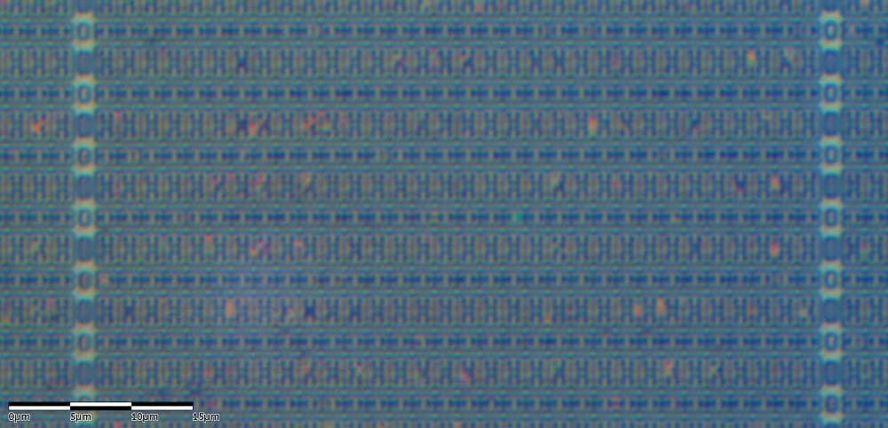
Le schéma intégré montre comment un bit de mémoire statique se maintient lui-même : une boucle de deux inverseurs. La macro de cet échelon est constituée de 4 096 bits de mémoire statique dans un seul réseau.
3

Les broches de la macro, et trois choses que son modèle indique

gf180mcu_fd_ip_sram__sram512x8m8wm1 contient 512 octets. Ses broches : CLK ; A, une adresse de 9 bits ; D, l'octet à écrire ; Q, l'octet lu. Les trois commandes sont toutes actives à LOW. CEN à 0 met la mémoire sous tension. GWEN à 0 fait du front d'horloge une écriture, à 1 une lecture. WEN comporte un bit par bit de donnée, et un 0 permet l'écriture de ce bit ; une écriture peut donc modifier certains bits d'un octet et laisser les autres inchangés. La lecture du modèle de simulation de PDK révèle trois points utiles à connaître. Premièrement, la mémoire ne fonctionne qu'après que CEN est passé de 1 à 0 ; sinon le modèle affiche « CEN is not reset, memory is not operational », donc le cœur maintient CEN à 1 pendant la réinitialisation et le baisse ensuite. Deuxièmement, une lecture donne mem[A] sur Q juste après le front d'horloge ayant échantillonné A, donc la donnée est prête un cycle d'horloge plus tard. Troisièmement, le modèle démarre avec chaque octet à 0. Une puce réelle ne le fait pas : sa SRAM se met sous tension avec la valeur dans laquelle chaque cellule s'est retrouvée, donc la conception doit écrire avant de lire. L'exemple du template lie CEN à 1, donc ses deux macros restent désactivées. Ses fichiers de temporisation donnent la période d'horloge minimale de la macro comme 6,6 ns dans le coin typique à 5 V et 18,3 ns dans le coin lent à 3,0 V, 125 °C, toutes deux bien en deçà des 40 ns du template.
4

The core

src/chip_core.sv for the pattern player, with the template's port list unchanged plus one parameter, HOLD_LOG2. Input pad 0 enables, pad 1 selects LOAD mode, pad 2 is the write strobe; bidirectional pads 0 to 7 carry the byte, pad 8 the PWM. The LOAD and strobe pads are passed through two flip-flops before use, a synchroniser: they change whenever the outside world likes, not in step with the chip's clock, and a flip-flop caught mid-change can hover between 0 and 1 for a while. In play mode, each time HOLD_LOG2 periods have passed, the byte the SRAM has been reading becomes the new duty and the address moves on.
chip_core.svsystemverilog
// SPDX-License-Identifier: Apache-2.0
// Youblob silicon rung 5: the PWM dimmer plays a brightness pattern stored in the on-chip SRAM macro.
// Port list unchanged from wafer-space/gf180mcu-project-template src/chip_core.sv.

`default_nettype none

module chip_core #(
    parameter NUM_INPUT_PADS,
    parameter NUM_BIDIR_PADS,
    parameter NUM_ANALOG_PADS,
    parameter HOLD_LOG2 = 9        // each table entry lasts 2**HOLD_LOG2 PWM periods
    )(
    `ifdef USE_POWER_PINS
    inout  wire VDD,
    inout  wire VSS,
    `endif

    input  wire clk,       // clock
    input  wire rst_n,     // reset (active low)

    input  wire [NUM_INPUT_PADS-1:0] input_in,   // Input value
    output wire [NUM_INPUT_PADS-1:0] input_pu,   // Pull-up
    output wire [NUM_INPUT_PADS-1:0] input_pd,   // Pull-down

    input  wire [NUM_BIDIR_PADS-1:0] bidir_in,   // Input value
    output wire [NUM_BIDIR_PADS-1:0] bidir_out,  // Output value
    output wire [NUM_BIDIR_PADS-1:0] bidir_oe,   // Output enable
    output wire [NUM_BIDIR_PADS-1:0] bidir_cs,   // Input type (0=CMOS Buffer, 1=Schmitt Trigger)
    output wire [NUM_BIDIR_PADS-1:0] bidir_sl,   // Slew rate (0=fast, 1=slow)
    output wire [NUM_BIDIR_PADS-1:0] bidir_ie,   // Input enable
    output wire [NUM_BIDIR_PADS-1:0] bidir_pu,   // Pull-up
    output wire [NUM_BIDIR_PADS-1:0] bidir_pd,   // Pull-down

    inout  wire [NUM_ANALOG_PADS-1:0] analog  // Analog
);

    // Input pad 0: enable.  Input pad 1: LOAD mode.  Input pad 2: write strobe.
    // Bidir pads 0..7: the byte to store while loading.  Bidir pad 8: the PWM output.
    localparam DUTY_W = 8;
    localparam PWM_PAD = 8;

    assign input_pu = '0;
    assign input_pd = '0;
    assign bidir_oe = {{(NUM_BIDIR_PADS-DUTY_W){1'b1}}, {DUTY_W{1'b0}}};
    assign bidir_ie = ~bidir_oe;
    assign bidir_cs = {{(NUM_BIDIR_PADS-DUTY_W){1'b0}}, {DUTY_W{1'b1}}};
    assign bidir_sl = '0;
    assign bidir_pu = '0;
    assign bidir_pd = '0;

    wire enable = input_in[0];
    wire [DUTY_W-1:0] data_in = bidir_in[DUTY_W-1:0];

    // The mode and strobe pads change whenever the outside world likes, not in step with clk:
    // two flip-flops in a row (a synchroniser) before anything uses them.
    logic [1:0] load_s;
    logic [2:0] strobe_s;
    always_ff @(posedge clk) begin
        load_s   <= {load_s[0], input_in[1]};
        strobe_s <= {strobe_s[1:0], input_in[2]};
    end
    logic load_was;
    wire load        = load_s[1];
    wire load_start  = load & ~load_was;
    wire strobe_rise = strobe_s[1] & ~strobe_s[2];
    always_ff @(posedge clk) load_was <= load;

    // The SRAM wants its chip enable (CEN, active LOW) to go 1 -> 0 before it works:
    // hold it at 1 through reset, then 0.
    logic cen;
    always_ff @(posedge clk) cen <= !rst_n;

    // PWM counter and the "hold" counter that decides when to step to the next table entry.
    logic [DUTY_W-1:0] count;
    logic [HOLD_LOG2:0] hold;                   // one bit wider so HOLD_LOG2 = 0 still works
    wire period_end = (count == '1);
    localparam logic [HOLD_LOG2:0] HOLD_MASK = (1 << HOLD_LOG2) - 1;   // 0 when HOLD_LOG2 = 0
    wire step = period_end && ((hold & HOLD_MASK) == HOLD_MASK);

    logic [DUTY_W-1:0] addr;
    logic [DUTY_W-1:0] duty;
    wire  [DUTY_W-1:0] q;                       // SRAM read data: mem[addr], one clock after addr

    always_ff @(posedge clk) begin
        if (!rst_n) begin
            count <= '0;  hold <= '0;  addr <= '0;  duty <= '0;
        end else if (load) begin
            count <= '0;  hold <= '0;  duty <= '0;
            if (load_start)       addr <= '0;       // every load starts at entry 0
            else if (strobe_rise) addr <= addr + 1'b1;
        end else if (enable) begin
            count <= count + 1'b1;
            if (period_end) hold <= hold + 1'b1;
            if (step) begin
                duty <= q;                          // the entry that was being read
                addr <= addr + 1'b1;                // and move on to the next
            end
        end
    end

    `gf180mcu_xxx_ip_sram__sram512x8m8wm1 sram_0 (
        `ifdef USE_POWER_PINS
        .VDD  (VDD),
        .VSS  (VSS),
        `endif
        .CLK  (clk),
        .CEN  (cen),                                   // active low: 0 = on
        .GWEN (~(load && strobe_rise)),                // active low: 0 = write this clock
        .WEN  (8'b0),                                  // active low, per bit: write all eight
        .A    ({1'b0, addr}),                          // 256 of the 512 bytes
        .D    (data_in),
        .Q    (q)
    );

    logic pwm;
    always_ff @(posedge clk) begin
        if (!rst_n) pwm <= 1'b0;
        else        pwm <= enable && !load && (count < duty);
    end

    logic [NUM_BIDIR_PADS-1:0] out;
    always_comb begin
        out = '0;
        out[PWM_PAD] = pwm;
    end
    assign bidir_out = out;

    // Inputs this design does not read (keeps lint quiet, as the template does with _unused).
    logic _unused;
    assign _unused = &{1'b0, input_in[NUM_INPUT_PADS-1:3], bidir_in[NUM_BIDIR_PADS-1:DUTY_W], hold[HOLD_LOG2]};

endmodule

`default_nettype wire

Outils nécessaires :

Ordinateur de bureauOrdinateur de bureau
5

The test

test_pattern.py builds the core with the PDK's SRAM model, gf180mcu_fd_ip_sram__sram512x8m8wm1.v, at the template's 25 MHz and with HOLD_LOG2 = 0 so the whole table plays in 256 periods. It loads the table through the pads the way the ESP32 will, then counts the high clocks in each of 600 PWM periods and requires them to follow the table from exactly one starting point. A second test loads again and checks the new pattern replaced the old.
test_pattern.pypython
# SPDX-License-Identifier: Apache-2.0
# cocotb testbench for the SRAM pattern player, with the PDK's own SRAM simulation model
# (gf180mcu_fd_ip_sram__sram512x8m8wm1, gf180mcuD, the commit the template pins).
import math
import os
from pathlib import Path

import cocotb
from cocotb.clock import Clock
from cocotb.triggers import ClockCycles, FallingEdge, RisingEdge
from cocotb_tools.runner import get_runner

PWM_PAD = 8
EN, LOAD, STROBE = 1, 2, 4                      # input pad bits
SRAM = Path(os.getenv("PDK_ROOT", "pdk")) / "gf180mcuD" / "libs.ref" / "gf180mcu_fd_ip_sram" / "verilog"


def breathing_table(n=256, gamma=2.2):
    """One slow breath: a raised sine, gamma-corrected so equal steps LOOK equal to the eye."""
    return [round(255 * ((1 - math.cos(2 * math.pi * i / n)) / 2) ** gamma) for i in range(n)]


async def start(dut):
    cocotb.start_soon(Clock(dut.clk, 40, unit="ns").start())   # 25 MHz, the template's CLOCK_PERIOD
    dut.input_in.value = 0
    dut.bidir_in.value = 0
    dut.rst_n.value = 0
    await ClockCycles(dut.clk, 5)
    dut.rst_n.value = 1
    await ClockCycles(dut.clk, 2)


async def load(dut, table):
    """What a microcontroller on the breakout does: LOAD high, then per byte set the data pads,
    raise the strobe, wait, lower it. The chip synchronises the strobe, so hold each for 4 clocks."""
    dut.input_in.value = LOAD
    await ClockCycles(dut.clk, 4)
    for b in table:
        dut.bidir_in.value = b
        await ClockCycles(dut.clk, 1)
        dut.input_in.value = LOAD | STROBE
        await ClockCycles(dut.clk, 4)
        dut.input_in.value = LOAD
        await ClockCycles(dut.clk, 4)
    dut.input_in.value = 0
    await ClockCycles(dut.clk, 4)


async def highs_per_period(dut, periods):
    """High clocks in each PWM period, counted from the core's own count = 0."""
    while int(dut.count.value) != 0:
        await RisingEdge(dut.clk)
    out = []
    for _ in range(periods):
        n = 0
        for _ in range(256):
            await FallingEdge(dut.clk)
            n += int(dut.bidir_out.value[PWM_PAD])
        out.append(n)
    return out


@cocotb.test()
async def test_plays_the_table(dut):
    """Load a 256-entry breathing table, play it: each period's high time is the next entry."""
    table = breathing_table()
    await start(dut)
    await load(dut, table)
    dut.input_in.value = EN
    got = await highs_per_period(dut, 600)
    # the output starts part-way through the table; find where, then demand every period match
    fits = [off for off in range(256) if all(got[j] == table[(j + off) % 256] for j in range(2, 600))]
    dut._log.info(f"first periods {got[:8]}, table aligns at offset {fits}")
    Path(__file__).resolve().parent.joinpath("pattern_trace.csv").write_text("\n".join(map(str, got)))
    assert len(fits) == 1, f"the output does not follow the table (offsets that fit: {fits})"


@cocotb.test()
async def test_reload(dut):
    """Loading again replaces the pattern: a flat 64 gives 64 high clocks every period."""
    await start(dut)
    await load(dut, breathing_table())
    await load(dut, [64] * 256)
    dut.input_in.value = EN
    got = await highs_per_period(dut, 40)
    assert all(g == 64 for g in got[2:]), got


def test_runner():
    here = Path(__file__).resolve().parent
    defines = {"gf180mcu_xxx_ip_sram__sram512x8m8wm1": "gf180mcu_fd_ip_sram__sram512x8m8wm1"}
    runner = get_runner("icarus")
    runner.build(
        sources=[SRAM / "gf180mcu_fd_ip_sram__sram512x8m8wm1.v", here / "chip_core.sv"],
        hdl_toplevel="chip_core",
        parameters={"NUM_INPUT_PADS": 4, "NUM_BIDIR_PADS": 38, "NUM_ANALOG_PADS": 4, "HOLD_LOG2": 0},
        defines=defines,
        build_args=["-g2012"],
        timescale=("1ns", "1ps"),
        always=True,
    )
    runner.test(hdl_toplevel="chip_core", test_module="test_pattern")


if __name__ == "__main__":
    test_runner()

Outils nécessaires :

Ordinateur de bureauOrdinateur de bureau
6

Ce que la simulation a affiché

Exécution de ce blueprint avec Icarus Verilog 12.0 et cocotb 2.1.0 : -------- MESSAGE: CEN vient d’être réinitialisé, la mémoire est opérationnelle --------- test_pattern.test_plays_the_table PASS (600 périodes, la table s’aligne à exactement un décalage) test_pattern.test_reload PASS TESTS=2 PASS=2 FAIL=0 SKIP=0 Pour prouver que le test peut échouer, WEN a été modifié de 8'b0 à 8'hFF : l’erreur classique avec une broche active à l’état bas, chaque bit masqué, rien d’écrit, une table de zéros. Les deux tests ont échoué, et le cœur a été remis en place. La première ligne est le message propre au modèle SRAM : le cœur a abaissé CEN après la réinitialisation, comme le modèle l’exige.
7

Load it from an ESP32

Once the chip is on its breakout board, this sketch writes the table. Eight GPIOs carry the byte, three more drive LOAD, the strobe and enable, and an LED with a 330 ohm resistor from pad 8 to ground shows the breath. Each level is held for 1 microsecond, 25 of the chip's clocks, so the synchroniser always sees it. The sketch then does nothing: the pattern lives in the chip. It is lost when the chip loses power, so send r over serial to load it again. The ESP32 is a 3.3 V part and its inputs are not 5 V tolerant. The sketch only drives the chip and never reads from it. The template's default libraries are the 5 V ones; before you connect, check in the I/O library's documentation that 3.3 V is a valid logic high for your chip's inputs, or build with the 3.3 V libraries, as the template's README shows. The sketch compiles for the ESP32 with the Arduino ESP32 core 3.3.12; it has not been run, because the chip does not exist yet.
load_pattern.inocpp
// SPDX-License-Identifier: Apache-2.0
// Load a breathing pattern into your chip's SRAM through its pads, then let the chip play it.
// Youblob silicon rung 5. The chip does the playing; this board only writes 256 bytes once.
//
// Wiring (ESP32 GPIO -> chip pad on your breakout):
//   D0..D7  GPIO 13,14,18,19,21,22,23,25 -> bidir[0..7]
//   LOAD    GPIO 26 -> input[1]
//   STROBE  GPIO 27 -> input[2]
//   EN      GPIO 32 -> input[0]
//   and a common ground. The chip's bidir[8] drives an LED through 330 ohm to ground.
// The ESP32 is a 3.3 V part: run the chip's I/O at 3.3 V, or put a level shifter between them.

#include <math.h>

const int DATA_PINS[8] = {13, 14, 18, 19, 21, 22, 23, 25};
const int PIN_LOAD = 26, PIN_STROBE = 27, PIN_EN = 32;

// The chip passes LOAD and STROBE through a two-flip-flop synchroniser and looks for the strobe's
// rising edge, so every level has to last a few of ITS clocks. 1 us is 25 clocks at 25 MHz.
const unsigned HOLD_US = 1;

uint8_t table[256];

void makeBreathingTable() {
  // a raised sine, gamma-corrected (2.2) so the brightness steps look even to the eye
  for (int i = 0; i < 256; i++) {
    float s = (1.0f - cosf(2.0f * PI * i / 256.0f)) / 2.0f;
    table[i] = (uint8_t)lroundf(255.0f * powf(s, 2.2f));
  }
}

void putByte(uint8_t b) {
  for (int bit = 0; bit < 8; bit++) digitalWrite(DATA_PINS[bit], (b >> bit) & 1);
  delayMicroseconds(HOLD_US);            // data settles before the strobe
  digitalWrite(PIN_STROBE, HIGH);        // the chip writes on the strobe's rising edge...
  delayMicroseconds(HOLD_US);            // ...a few of its clocks later, so hold the data
  digitalWrite(PIN_STROBE, LOW);
  delayMicroseconds(HOLD_US);
}

void loadTable() {
  digitalWrite(PIN_EN, LOW);
  digitalWrite(PIN_LOAD, HIGH);          // entering LOAD resets the chip's address to 0
  delayMicroseconds(HOLD_US);
  for (int i = 0; i < 256; i++) putByte(table[i]);
  digitalWrite(PIN_LOAD, LOW);
  delayMicroseconds(HOLD_US);
}

void setup() {
  Serial.begin(115200);
  for (int bit = 0; bit < 8; bit++) pinMode(DATA_PINS[bit], OUTPUT);
  pinMode(PIN_LOAD, OUTPUT);
  pinMode(PIN_STROBE, OUTPUT);
  pinMode(PIN_EN, OUTPUT);
  digitalWrite(PIN_STROBE, LOW);

  makeBreathingTable();
  loadTable();
  digitalWrite(PIN_EN, HIGH);            // play
  Serial.println("pattern loaded; the chip is playing it on its own");
  Serial.printf("table[0]=%u table[64]=%u table[128]=%u\n", table[0], table[64], table[128]);
}

void loop() {
  // Nothing to do: the pattern lives in the chip's SRAM now.
  // Send 'r' over serial to load it again (the SRAM loses it when the chip loses power).
  if (Serial.available() && Serial.read() == 'r') {
    loadTable();
    digitalWrite(PIN_EN, HIGH);
    Serial.println("reloaded");
  }
}

Matériaux pour cette étape :

Puce ASIC sur mesurePuce ASIC sur mesure1 pièce
Circuit impriméCircuit imprimé1 pièce
LED 5 mmLED 5 mm1 pièce
Résistance de 330 ohmsRésistance de 330 ohms1 pièce

Outils nécessaires :

Carte de développement ESP32Carte de développement ESP32
Plaque d'essaiPlaque d'essai
Fils de liaisonFils de liaison
Ordinateur de bureauOrdinateur de bureau
8

Un motif qui ne se stocke pas ou ne se lit pas

Dépannage du motif SRAM.

Flow

Loading...
9

Sources et limites honnêtes

**Sources**, consultées le 29 septembre 2026 : le GF180MCU PDK au commit épinglé par le modèle (gf180mcuD, f6eeac7dad085ffcc829ccfd721f7b4ce39edcf7, issu des releases ciel de fossi-foundation ; Apache-2.0) : le modèle SRAM gf180mcu_fd_ip_sram__sram512x8m8wm1.v, son LEF pour le contour et ses fichiers de temporisation pour la période d'horloge minimale ; le fichier de temporisation bibliothèque de cellules standard pour la surface des bascules. Le dépôt wafer-space/gf180mcu-project-template (src/chip_core.sv, src/chip_top.sv, README.md, librelane/config.yaml ; Apache-2.0). **Limites honnêtes.** La simulation est au niveau chip_core, avec le modèle propre au SRAM, mais sans l'anneau de plots, la synthèse ni le placement-routage, et les vérifications de temporisation du modèle ne tranchent rien ici. Le croquis ESP32 a été compilé, pas exécuté. HOLD_LOG2 valait 0 dans le test afin qu'il se termine ; la puce utiliserait 9, un souffle d'environ 1,3 s.

Matériaux

4

Outils requis

4

CC0 Domaine public

Ce blueprint est publié sous CC0. Vous êtes libre de copier, modifier, distribuer et utiliser ce travail pour tout usage, sans demander la permission.

Soutenez le Maker en achetant des produits via son Blueprint où il perçoit une Commission Maker définie par les Vendeurs, ou créez une nouvelle itération de ce Blueprint et incluez-le comme connexion dans votre propre Blueprint pour partager les revenus.

Commentaires

(0)

Se connecter pour participer à la discussion

Chargement des commentaires...