ART
BEAUTÉ ET BIEN-ÊTRE
ARTISANAT
CULTURE ET HISTOIRE
DIVERTISSEMENT
ENVIRONNEMENT
NOURRITURE ET BOISSONS
INGÉNIERIE INVERSE
SCIENCES
SPORTS
TECHNOLOGIE
TECHNOLOGIE PORTABLE
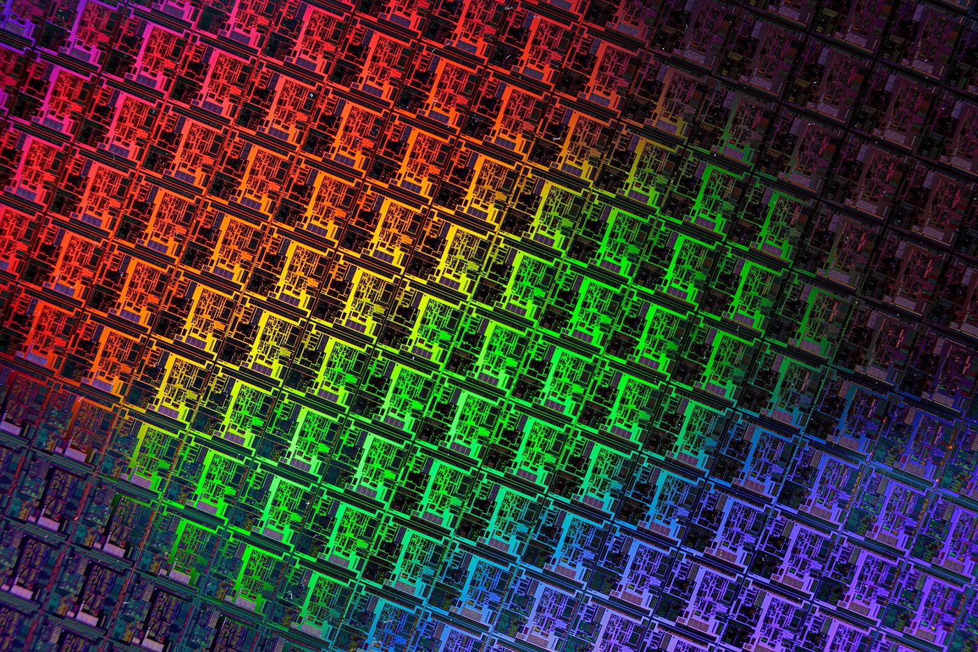


Thermal Oxidation and the Oxide Mask
Silicon rusts, and that turns out to be the most valuable accident in the history of manufacturing.
Heat silicon in oxygen and it grows a layer of silicon dioxide — glass — on its surface. Unlike the flaking rust on iron, this oxide is dense, hard, chemically inert, an excellent electrical insulator, and it bonds to the silicon beneath it so intimately that the interface between them has remarkably few electrically active defects. Germanium, the material the transistor was invented on, has no equivalent: germanium oxide is soft, and it dissolves in water.
That single material property is why the entire industry runs on silicon rather than germanium, despite germanium having better carrier mobility.
But the property that mattered most was not discovered until 1955, and it was found by accident. Carl Frosch and Lincoln Derick at Bell Labs were diffusing dopants into silicon and kept ruining samples until a hydrogen carrier gas caught fire in the furnace, introducing water vapour, which grew a thick oxide. The oxidised samples came out intact — and, on examination, the dopant had not penetrated where the oxide covered the surface. They published it in 1957.
The oxide was a MASK. Dopants diffuse through silicon readily at 1000 degrees and through silicon dioxide far more slowly, so a patterned oxide layer says here and not here to a diffusion that would otherwise go everywhere. Cut a hole in the oxide, and the dopant enters through the hole and nowhere else.
That is the foundation of every integrated circuit ever made. Not the transistor — the ability to decide WHERE the transistor is.
A diffusion furnace is not bench equipment. What you will do here is grow a real, measurable oxide by anodising, measure its thickness by its own interference colours, and prove it masks — using a process you can run on a kitchen table that shares the essential physics.
Intermédiaire
4 hours
Consignes
1
1
Grow an oxide you can measure, and read its thickness in colour
Grow an oxide you can measure, and read its thickness in colour
You cannot run a 1000 degree oxidation furnace. You can grow a dense, adherent, insulating oxide of controlled thickness by anodising aluminium, and the measurement technique you will use on it is precisely the one used on silicon dioxide.
WHY ALUMINIUM IS AN HONEST STAND-IN, AND WHERE IT IS NOT. Anodised aluminium oxide is like thermal silicon dioxide in the ways that matter for this exercise: it grows from the substrate rather than being deposited on it, so it consumes the metal beneath as it thickens; it is a hard insulator; its thickness is controllable and repeatable; and it shows the same optical interference colours. It differs in that it is grown electrochemically at room temperature rather than thermally, it is porous unless sealed, and it is not a dopant mask in the semiconductor sense. State that difference to anyone you show this to.
THE SETUP. A strip of clean aluminium as the anode, a lead or aluminium cathode, and a bath of dilute sulfuric acid — 10 to 15 percent by volume — at room temperature. A bench power supply at 12 to 20 volts, current limited to about 1 amp per square decimetre of anode area. Wear goggles and gloves; this is dilute acid but it is still acid, and hydrogen comes off the cathode so keep it ventilated and away from flames.
Degrease the aluminium first in warm detergent, rinse, then dip briefly in dilute sodium hydroxide to strip the native oxide, and rinse again. Handle by the edges from that point. Contamination shows up as patchy colour.
THE MEASUREMENT, AND IT IS THE INTERESTING PART. Run the anodising for a set time, rinse, and look at the strip in daylight. It will be coloured — and the colour is not a dye, it is a THICKNESS MEASUREMENT. Light reflecting off the top surface of the oxide interferes with light that travelled down through the oxide and reflected off the metal beneath. Whether they add or cancel depends on the extra distance travelled, which is twice the oxide thickness times its refractive index. Some wavelengths cancel; the rest is the colour you see.
This is exactly how a fab engineer reads oxide thickness on a silicon wafer at a glance. There is a standard colour chart for silicon dioxide on silicon, and an experienced eye reads it to within about 10 nanometres without any instrument at all.
Run four strips at 2, 5, 10 and 20 minutes, all other conditions identical. Photograph them together on a neutral background under the same light. You should get a clear progression through the interference series, and the notebook will turn those colours back into thicknesses so you can plot growth against time.
Matériaux pour cette étape :
 Plat en aluminium1 metre
 Acide sulfurique1 litre
 Hydroxyde de sodium — qualité laboratoire100 gram
 Feuille de plomb1 pièce
 Eau distillée5 litres
Outils nécessaires :
 Alimentation de laboratoire
 Multimètre numérique de laboratoire
 Lunettes de sécurité de laboratoire
 Gants résistants aux produits chimiques
 Chronomètre
 Bécher en verre
2
2
Deal-Grove: why oxide growth slows down, and how much
Deal-Grove: why oxide growth slows down, and how much
Chargement du notebook Jupyter…
Outils nécessaires :
 Ordinateur de bureau
3
3
Prove the oxide masks — open a window and let something through
Prove the oxide masks — open a window and let something through
An oxide that merely sits there is a coating. An oxide that stops a process where it is present and permits it where it has been removed is a MASK, and that is the property the whole industry is built on. Prove it.
The demonstration uses electrochemical attack rather than dopant diffusion, because you cannot run a diffusion furnace — but the logic being tested is identical: patterned barrier, selective process, result confined to the openings.
PATTERN THE OXIDE. Take one of your well-anodised strips. Mask part of it with nail varnish, wax crayon, or vinyl tape — anything that resists the etchant. Now strip the exposed oxide by immersing briefly in dilute sodium hydroxide, which dissolves aluminium oxide but leaves your resist alone. Thirty seconds is usually enough; watch for the colour to disappear from the unmasked area, which tells you the oxide is gone because the interference film has gone. Rinse thoroughly and remove the resist with acetone.
You now hold a strip with oxide in some places and bare metal in others, and you can SEE which is which from the colour. That is a patterned mask, and getting to this point is the entire content of the photolithography blueprint later in this chain — this version just uses a hand-applied resist instead of light.
NOW RUN A PROCESS AND SEE IF IT RESPECTS THE PATTERN. Dip the strip into a copper sulfate solution. Aluminium is well above copper in the electrochemical series, so bare aluminium displaces copper from solution and plates itself with a dark copper film within seconds. Anodised aluminium does not: the oxide is an insulator and a physical barrier, so no electron transfer occurs and no copper deposits.
Pull the strip out after a minute and rinse. The copper should appear ONLY in the windows you opened, with a sharp edge at the oxide boundary. Photograph it.
WHAT YOU HAVE DEMONSTRATED, PRECISELY. That a grown oxide can be selectively removed to define regions, and that a subsequent process then acts only in those regions. That is the mask principle, complete.
WHAT YOU HAVE NOT DEMONSTRATED, AND SAY SO. Frosch and Derick's discovery was specifically that silicon dioxide slows the DIFFUSION of dopant atoms through the solid — boron and phosphorus move through silicon dioxide hundreds to thousands of times more slowly than through silicon, so a few hundred nanometres of oxide holds back a diffusion that penetrates micrometres into the exposed silicon. Copper displacement is a surface electrochemical reaction, not solid-state diffusion. The masking GEOMETRY is the same; the physics being masked is not. Anyone who tells a student otherwise has taught them something false.
MEASURE THE EDGE. Look at the boundary under a microscope. How sharp is it? Your hand-applied resist probably gives a ragged edge tens or hundreds of micrometres wide. Note that number — it is your resolution, and improving it by four orders of magnitude is what the next fifteen years of the industry was about.
Matériaux pour cette étape :
Plat en aluminium1 metre Sulfate de cuivre (qualité laboratoire)200 gramHydroxyde de sodium — qualité laboratoire100 gram
 Acétone500 millilitre
 Ruban isolant1 pièce
Outils nécessaires :
 Microscope numériqueLunettes de sécurité de laboratoireGants résistants aux produits chimiquesBécher en verreChronomètre
4
4
Compendium — why silicon won, and what the oxide costs
Compendium — why silicon won, and what the oxide costs
WHY DID GERMANIUM LOSE? Germanium has higher electron and hole mobility than silicon, so on raw device speed it should have won. It lost on its oxide. Germanium dioxide is water-soluble — you cannot wash a wafer — and it is a poor insulator with a defective interface. Silicon's oxide is glass: insoluble, hard, an excellent dielectric, and it forms an interface with the silicon beneath that has remarkably few electrically active traps once hydrogen-annealed. Silicon also has a wider bandgap, so devices work at higher temperature. The industry chose the material with the better OXIDE, not the better semiconductor, and that tells you which property was actually binding.
WHY DOES THE SURFACE MOVE DOWNWARD AS THE OXIDE GROWS? Because the oxide consumes the silicon beneath it. Growing a layer of silicon dioxide of thickness d consumes about 0.44 d of silicon, and the oxide occupies more volume than the silicon it replaced, so roughly 56 percent of the final oxide stands above the original surface and 44 percent lies below it. This is not a curiosity: it is why oxidising over a patterned area produces the characteristic step, and why the field oxide in an integrated circuit is partly recessed into the wafer.
WHAT IS THE BIRD'S BEAK? When oxide grows in a window defined by a silicon nitride mask, oxygen also creeps sideways underneath the edge of the nitride, lifting it slightly and producing a tapering wedge of oxide shaped exactly like a bird's beak. It eats into the area you meant to keep clear, so the device is smaller than the mask said. For years it was one of the practical limits on packing density, and defeating it produced a small industry of process variants.
WHY DRY OXIDE FOR GATES AND WET FOR FIELD? Wet oxidation is about ten times faster because water diffuses through silicon dioxide far better than molecular oxygen does — but the resulting oxide is slightly less dense and has a worse interface. A gate oxide is thin, and everything about the transistor's behaviour depends on the quality of that interface, so it is grown dry and slowly. A field oxide is thick and merely has to insulate, so it is grown wet and quickly. The choice is made on purpose each time.
HOW THIN DID GATE OXIDES GET, AND WHAT STOPPED THEM? Down to about 1.2 nanometres, which is roughly five atomic layers. What stopped them was quantum mechanical tunnelling: below that, electrons pass straight through the insulator and the gate leaks badly enough to dominate the power budget. The answer was to abandon silicon dioxide for the gate and use a different insulator with a higher dielectric constant — hafnium-based oxides, from around 2007 — which gives the same capacitance from a physically thicker layer. Fifty years of the industry running on silicon's own oxide ended there, and it ended for a quantum reason rather than a manufacturing one.
WHAT DID FROSCH AND DERICK ACTUALLY UNLOCK? Selectivity. Before them, a diffusion went everywhere on the wafer and devices had to be separated by cutting the wafer up. After them, you could decide where. That is the difference between making transistors and making CIRCUITS of transistors, and it is why the planar process arrived two years later and the integrated circuit two years after that.
5
5
The oxide-mask cycle, and what it made possible
The oxide-mask cycle, and what it made possible
One diagram, because the sequence is the invention.
Before Frosch and Derick, a dopant diffusion covered the whole wafer. Devices were made one to a chip and separated by sawing, and there was no way to place two different doped regions in a chosen relationship to each other.
After them, the cycle below can be repeated. Grow oxide over everything, open a window where you want the dopant, diffuse, and the dopant enters through the window only. Then regrow oxide — which happens automatically during the diffusion itself, since the furnace is hot and oxygen is present — and open a different window somewhere else. Each pass places one more doped region, registered against the ones already there.
Repeat it three times and you have placed a collector, a base and an emitter in one piece of silicon, each inside the last, all sealed under glass. That is a planar transistor, and it is the next blueprint in this chain.
The diagram also shows the three ways the mask fails, because each is a real limit rather than a mistake: the oxide is a slow barrier and not an absolute one, so too long a diffusion penetrates it; dopant entering a window spreads sideways as well as down, so the doped region is always wider than the window; and every high-temperature step moves every dopant already placed.
Flow
Loading...
Matériaux
8- 1 metreEspace réservé
- 1 litreEspace réservé
- Espace réservé
- 1 pièceEspace réservé
- 5 litresEspace réservé
- Espace réservé
- 500 millilitreEspace réservé
- 1 pièceEspace réservé
Outils requis
8- Espace réservé
- Espace réservé
- Espace réservé
- Espace réservé
- Espace réservé
- Espace réservé
- Espace réservé
- Espace réservé
Blueprints liés
Ces blueprints partagent des connaissances — techniques, matériaux ou principes



CC0 Domaine public
Ce blueprint est publié sous CC0. Vous êtes libre de copier, modifier, distribuer et utiliser ce travail pour tout usage, sans demander la permission.
Soutenez le Maker en achetant des produits via son Blueprint où il perçoit une Commission Maker définie par les Vendeurs, ou créez une nouvelle itération de ce Blueprint et incluez-le comme connexion dans votre propre Blueprint pour partager les revenus.