SENI
KECANTIKAN & KESEHATAN
KERAJINAN
BUDAYA & SEJARAH
HIBURAN
LINGKUNGAN
MAKANAN & MINUMAN
REKAYASA BALIK
ILMU PENGETAHUAN
OLAHRAGA
TEKNOLOGI
PERANGKAT PAKAI

The Avalanche Photodiode Receiver
A fibre link is only as good as the weakest photon it can hear. After 80 km of glass a milliwatt launched at one end arrives as a few tens of nanowatts, and the question at the far end is not how to amplify light — it is where to put the gain so that you amplify the signal more than you amplify the noise.
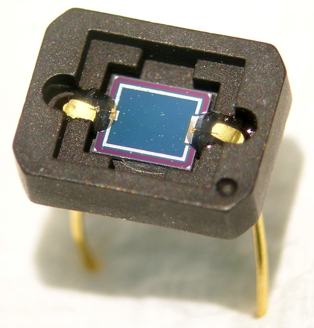
There are two places to put it, and they are genuine alternatives. A PIN photodiode has no gain at all and hands a tiny current to an amplifier that must supply everything; the amplifier's own thermal noise then sets the floor. An avalanche photodiode biases the junction hard enough that each photo-generated carrier knocks more carriers out of the lattice on its way across, giving an internal current gain of tens to hundreds BEFORE the amplifier sees anything.
That sounds like it should always win, and it does not. Avalanche multiplication is random, so it adds noise of its own, described by an excess noise factor F(M) that grows with the gain. Signal power rises as M squared; the multiplied shot noise rises as M squared times F(M), which is faster. So there is an OPTIMUM gain, past which more gain makes the receiver worse — and if the signal is already strong, an APD is worse than a PIN at any gain.
FULLY BUILDABLE. The transimpedance amplifier at the heart of this is the single most useful analogue circuit in optics, and you will build it, measure its gain-bandwidth behaviour against three feedback resistors, and confirm that it follows one over the square root of Rf rather than one over Rf. That difference is the entire reason the circuit exists.
Lanjutan
5 hours
Instruksi
1
1
Build the transimpedance amplifier
Build the transimpedance amplifier
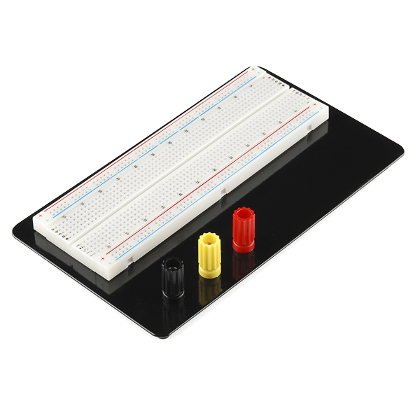
Build it on the breadboard, with R_F and C_F on sockets so you can swap them as a pair. Run the op-amp from two 9 V batteries as +9 V and -9 V. Reverse-bias the photodiode from the -9 V rail through R_BIAS and decouple the bias node with C_BIAS: reverse bias widens the depletion region and drops the BPW34's capacitance from about 72 pF to about 25 pF, and capacitance is what limits your bandwidth. The diode's cathode goes to the summing node, so the photocurrent flows out of it and the output rises with the light: V_OUT = + I_ph x R_F.
Keep the summing node, the wire from the diode to the inverting input, as short as physically possible. It is a high-impedance node and every picofarad of stray capacitance on it costs bandwidth and stability.
C_F is not decoration. With C_in on the summing node the loop has a pole inside it. C_F = sqrt(C_in / (2 pi R_F GBW)) gives 11.5 pF for 10k, 3.6 pF for 100k and 1.2 pF for 1M with C_in = 25 pF and a TL071 (GBW 3 MHz). Checked in ngspice with a behavioural TL071-class op-amp: with 1M and 1.2 pF the -3 dB point is 170 kHz and a step overshoots about 15 %; without C_F the response has a +27 dB resonant peak. So on the scope, 10 to 15 % overshoot on the edge is right, and a decaying oscillation means C_F is too small.
Memuat penampil KiCanvas...
Penampil desain PCB profesional
Material untuk langkah ini:
 Fotodioda (BPW34)1 buah
 Penguat operasional JFET (TL071)1 buah
 Set Resistor1 buah
 Set Kapasitor1 buah
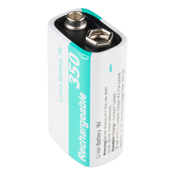 9V Li-ion Rechargeable Battery - 350mAh2 buah
 Dudukan baterai2 buah
Alat yang dibutuhkan:
 Breadboard - Classic
 Set Kabel Jumper
 Osiloskop Digital
 Multimeter Digital Kelas Laboratorium
2
2
Measure the bandwidth from the rise time
Measure the bandwidth from the rise time
Point the test LED at the photodiode across a small gap, or couple the two through a short plastic fibre, and flash it with the sketch below: the ESP32's LEDC peripheral makes a 1 kHz square wave in hardware, so its edges are exact. Put the scope on the SCOPE point and measure the 10-90 % rise time of the output edge for each R_F / C_F pair. The -3 dB bandwidth is about 0.35 divided by the rise time.
What the simulation predicts: 0.26 us (about 1.4 MHz) with 10k, 0.66 us (about 530 kHz) with 100k, 1.95 us (about 180 kHz) with 1M. Ten times the gain costs about three times the bandwidth, not ten times. If it costs ten, C_F is wrong or you have built a load resistor by leaving the op-amp out of the loop. With 10k the LED's own switching time can be part of what you measure, so trust the 100k and 1M pair most.
The sketch was compiled for the ESP32 with the Arduino ESP32 core 3.3.12. An earlier version of this step swept the LED with software delays and read the output with the ESP32's ADC; that could not keep time at the high frequencies, and the ADC cannot read the amplifier's output edge, so the scope does the measuring now.
tia_square_source.inocpp
Material untuk langkah ini:
 Kit LED1 buahSet Resistor1 buah
 Berkas serat optik1 meter
Alat yang dibutuhkan:
 Papan Pengembangan ESP32Breadboard - ClassicSet Kabel JumperOsiloskop Digital
 Komputer Desktop
3
3
Bias the avalanche photodiode
Bias the avalanche photodiode
Swap the BPW34 for the silicon APD, keeping everything else the same. An APD needs typically 100 to 200 V of reverse bias — check YOUR device's datasheet, because the breakdown voltage is a per-part number and exceeding it destroys the diode.
Use an adjustable high-voltage bench supply in place of the -9 V bias, with the APD's anode to its negative output, and current-limit it hard, to a few tens of microamps. At 100 to 200 V the bias is dangerous to touch: switch it off and let it discharge before changing anything. An APD in breakdown draws runaway current and dies in milliseconds; the series R_BIAS is the only thing standing between a mistake and a dead part.
Sweep the bias from 50 V upward in 5 V steps with a constant light level, and record the output at each. The photocurrent will be flat, then start to climb, then climb steeply. That curve IS the gain M against voltage, normalised to the flat region where M = 1.
Now warm the diode gently with your fingers and watch the output FALL at constant bias. APD gain drops as temperature rises, because hotter carriers scatter off lattice vibrations before they gain enough energy to ionise. That is why a real APD receiver servos its bias against a thermistor.
Material untuk langkah ini:
 Fotodioda longsoran (silikon)1 buahSet Resistor1 buah
Alat yang dibutuhkan:
 Sumber searah tegangan tinggi (meja kerja)Multimeter Digital Kelas LaboratoriumOsiloskop DigitalBreadboard - Classic
4
4
Gain-bandwidth, excess noise, and the optimum M
Gain-bandwidth, excess noise, and the optimum M
Memuat notebook Jupyter…
Alat yang dibutuhkan:
Komputer Desktop5
5
Compendium: PIN against APD, and where each one wins
Compendium: PIN against APD, and where each one wins
HOW MULTIPLICATION WORKS. In a high field a carrier gains enough energy between collisions to break a bond and make a new electron-hole pair; both accelerate and can do it again. M is the average number of carriers collected per carrier generated. The randomness of WHERE each ionisation happens is what makes the output noisier than simple shot noise.
WHY k IS THE MATERIAL'S WHOLE STORY. If only one carrier type ionises, the cascade runs one way and the statistics are tight. If both do, it feeds back on itself, the gain becomes wildly variable and F(M) heads towards M. Silicon k is about 0.02, InGaAs/InP about 0.45, germanium close to 0.9. Silicon APDs are superb — and silicon is transparent above about 1100 nm, exactly where fibre wants to work. The best APD material and the best fibre wavelength do not overlap, which is one reason the amplifier in the next blueprint mattered so much.
THE SIBLING TABLE. PIN photodiode: gain 1, no high-voltage supply, no temperature servo, flat response, cheap; all the gain and all the noise come from the amplifier. APD: gain 10 to 200, needs 100-200 V current-limited and temperature-compensated, adds F(M) of its own, and buys typically 5 to 10 dB of sensitivity in a thermally limited receiver — at a best M that is not the biggest M. The deciding question is never which is better, it is whether the receiver is THERMALLY LIMITED. If it is, the APD wins by putting its gain ahead of the thermal noise. If the signal is strong enough that shot noise already dominates, the APD only adds F(M) and makes things worse.
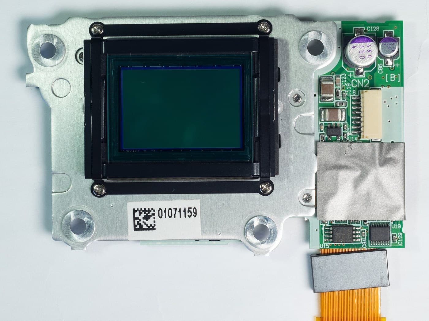
WHAT THIS SHARES WITH THE CCD. Both are silicon collecting photo-generated charge. The CCD integrates it in a capacitor for milliseconds then shifts it out; this receiver reads the current continuously at a hundred megahertz. Long integration against wide bandwidth, from identical physics — which is why a camera sensor can see a single star and cannot carry a gigabit.
COMMON FAILURES. Ringing on the step response means Cf is too small or the summing node is too long. A DC offset that swamps everything is ambient light, not a fault: AC-couple after the amplifier or put an optical filter in front. A dead APD is almost always a bias supply that was not current-limited.
Bahan
9- 1 buahPlaceholder
- Placeholder
- mulai$5.64
- 1 buahPlaceholder
- 9V Li-ion Rechargeable Battery - 350mAhkomisi 10%2 buah$5.64
- mulai$1.18
- 1 buahPlaceholder
- 1 meterPlaceholder
- Placeholder
Alat yang Diperlukan
7- Breadboard - Classickomisi 10%$9.43
- Placeholder
- Osiloskop Digitalkomisi 10%Magento Legacy Storeships internationallyPlaceholder
- Placeholder
- Placeholder
- Placeholder
- Placeholder
Estimasi total
Yang dibeli pembuatnya. Bahan tanpa harga didapat di tempat kamu membelinya.
Blueprint terkait
Blueprint ini berbagi pengetahuan — teknik, bahan, atau prinsip

CC0 Domain Publik
Cetak biru ini dirilis di bawah CC0. Anda bebas untuk menyalin, memodifikasi, mendistribusikan, dan menggunakan karya ini untuk tujuan apa pun, termasuk komersial, tanpa meminta izin.
Dukung Maker dengan membeli produk melalui Cetak Biru mereka di mana mereka mendapatkan Komisi Pembuat yang ditetapkan oleh Penjual, atau buat iterasi baru dari Cetak Biru ini dan masukkan sebagai koneksi di milik Anda sendiri.