SENI
KECANTIKAN & KESEHATAN
KERAJINAN
BUDAYA & SEJARAH
HIBURAN
LINGKUNGAN
MAKANAN & MINUMAN
REKAYASA BALIK
ILMU PENGETAHUAN
OLAHRAGA
TEKNOLOGI
PERANGKAT PAKAI

Youblob (simulation output) · CC0

The On-Chip SRAM: A Breathing Light Stored in Your Chip's Own Memory
wafer.space's template ships with two SRAM macros in its example design, 512 bytes each, and leaves them switched off. A macro is a finished block of memory from the PDK: 4,096 static memory cells, drawn once with their address decoder and read circuits, that you place whole instead of building from gates.
This rung switches one on. The PWM dimmer from the earlier rung now plays a pattern: a microcontroller writes 256 bytes into the chip through its pads, once, and from then on the chip reads them back by itself, one byte per step, as the brightness of a slowly breathing light.
The core and its testbench were run for this blueprint with Icarus Verilog 12.0, cocotb 2.1.0 and the PDK's own simulation model of the SRAM macro: the output followed the stored table for 600 PWM periods. The picture is that simulation's own output, one bar per period. The ESP32 sketch that loads the table was compiled for this blueprint; there is no chip yet to run it on.
Lanjutan
An evening, plus the chip
Instruksi
1
1
The pattern, the timing and the size
The pattern, the timing and the size
Memuat notebook Jupyter…
2
2
What each of the 4,096 bits is
What each of the 4,096 bits is
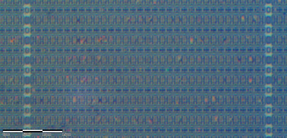
The embedded blueprint shows how one bit of static memory holds itself: a loop of two inverters. The macro in this rung is 4,096 bits of static memory in one array.
3
3
The macro's pins, and three things its model says
The macro's pins, and three things its model says
gf180mcu_fd_ip_sram__sram512x8m8wm1 holds 512 bytes. Its pins: CLK; A, a 9-bit address; D, the byte to write; Q, the byte read. The three controls are all active LOW. CEN at 0 switches the memory on. GWEN at 0 makes the clock edge a write, at 1 a read. WEN is one bit per data bit, and a 0 lets that bit be written, so a write can change some bits of a byte and leave the others alone.
Reading the PDK's simulation model shows three things worth knowing. First, the memory only works after CEN has gone from 1 to 0; the model prints "CEN is not reset, memory is not operational" otherwise, so the core holds CEN at 1 through reset and lowers it after. Second, a read gives mem[A] on Q just after the clock edge that sampled A, so the data is ready one clock later. Third, the model starts with every byte at 0. A real chip does not: its SRAM powers up holding whatever each cell fell into, so the design must write before it reads.
The template's own example ties CEN to 1, so its two macros sit switched off. Its timing files give the macro's minimum clock period as 6.6 ns at the typical 5 V corner and 18.3 ns at the slow 3.0 V, 125 °C corner, both well inside the template's 40 ns.
4
4
The core
The core
src/chip_core.sv for the pattern player, with the template's port list unchanged plus one parameter, HOLD_LOG2. Input pad 0 enables, pad 1 selects LOAD mode, pad 2 is the write strobe; bidirectional pads 0 to 7 carry the byte, pad 8 the PWM. The LOAD and strobe pads are passed through two flip-flops before use, a synchroniser: they change whenever the outside world likes, not in step with the chip's clock, and a flip-flop caught mid-change can hover between 0 and 1 for a while. In play mode, each time HOLD_LOG2 periods have passed, the byte the SRAM has been reading becomes the new duty and the address moves on.
chip_core.svsystemverilog
Alat yang dibutuhkan:
 Komputer Desktop
5
5
The test
The test
test_pattern.py builds the core with the PDK's SRAM model, gf180mcu_fd_ip_sram__sram512x8m8wm1.v, at the template's 25 MHz and with HOLD_LOG2 = 0 so the whole table plays in 256 periods. It loads the table through the pads the way the ESP32 will, then counts the high clocks in each of 600 PWM periods and requires them to follow the table from exactly one starting point. A second test loads again and checks the new pattern replaced the old.
test_pattern.pypython
Alat yang dibutuhkan:
Komputer Desktop6
6
What the simulation printed
What the simulation printed
Run for this blueprint with Icarus Verilog 12.0 and cocotb 2.1.0:
-------- MESSAGE: CEN is just reset, memory is operational ---------
test_pattern.test_plays_the_table PASS (600 periods, table aligns at exactly one offset)
test_pattern.test_reload PASS
TESTS=2 PASS=2 FAIL=0 SKIP=0
To prove the test can fail, WEN was changed from 8'b0 to 8'hFF, the classic slip with an active-low pin: every bit masked, nothing written, a table of zeros. Both tests failed, and the core was put back.
The first line is the SRAM model's own message: the core lowered CEN after reset, as the model requires.
7
7
Load it from an ESP32
Load it from an ESP32
Once the chip is on its breakout board, this sketch writes the table. Eight GPIOs carry the byte, three more drive LOAD, the strobe and enable, and an LED with a 330 ohm resistor from pad 8 to ground shows the breath. Each level is held for 1 microsecond, 25 of the chip's clocks, so the synchroniser always sees it. The sketch then does nothing: the pattern lives in the chip. It is lost when the chip loses power, so send r over serial to load it again.
The ESP32 is a 3.3 V part and its inputs are not 5 V tolerant. The sketch only drives the chip and never reads from it. The template's default libraries are the 5 V ones; before you connect, check in the I/O library's documentation that 3.3 V is a valid logic high for your chip's inputs, or build with the 3.3 V libraries, as the template's README shows. The sketch compiles for the ESP32 with the Arduino ESP32 core 3.3.12; it has not been run, because the chip does not exist yet.
load_pattern.inocpp
Material untuk langkah ini:
 Chip ASIC khusus1 buah
 Papan sirkuit cetak1 buah
 LED 5 mm1 buah
 Resistor 330 ohm1 buah
Alat yang dibutuhkan:
 Papan Pengembangan ESP32
 Breadboard - Classic
 Set Kabel JumperKomputer Desktop
8
8
A pattern that will not store or will not play
A pattern that will not store or will not play
SRAM pattern troubleshooting.
Flow
Loading...
9
9
Sources and honest limits
Sources and honest limits
**Sources**, read 29 September 2026: the GF180MCU PDK at the commit the template pins (gf180mcuD, f6eeac7dad085ffcc829ccfd721f7b4ce39edcf7, from the fossi-foundation ciel releases; Apache-2.0): the SRAM model gf180mcu_fd_ip_sram__sram512x8m8wm1.v, its LEF for the outline and its timing files for the minimum clock period; the standard-cell library's timing file for the flip-flop area. The wafer-space/gf180mcu-project-template repository (src/chip_core.sv, src/chip_top.sv, README.md, librelane/config.yaml; Apache-2.0).
**Honest limits.** The simulation is at the chip_core level, with the SRAM's own model but without the pad ring, synthesis or layout, and the model's timing checks do not decide anything here. The ESP32 sketch was compiled, not run. HOLD_LOG2 was 0 in the test so it would finish; the chip would use 9, a breath of about 1.3 s.
Bahan
4- 1 buahPlaceholder
- 1 buahPlaceholder
- 1 buahPlaceholder
Alat yang Diperlukan
4- Placeholder
- Placeholder
- Breadboard - Classickomisi 10%$9.43
- Placeholder
Blueprint terkait
Blueprint ini berbagi pengetahuan — teknik, bahan, atau prinsip


CC0 Domain Publik
Cetak biru ini dirilis di bawah CC0. Anda bebas untuk menyalin, memodifikasi, mendistribusikan, dan menggunakan karya ini untuk tujuan apa pun, termasuk komersial, tanpa meminta izin.
Dukung Maker dengan membeli produk melalui Cetak Biru mereka di mana mereka mendapatkan Komisi Pembuat yang ditetapkan oleh Penjual, atau buat iterasi baru dari Cetak Biru ini dan masukkan sebagai koneksi di milik Anda sendiri.