Collaborazione
ARTE
BELLEZZA E BENESSERE
MESTIERE
CULTURA E STORIA
DIVERTIMENTO
AMBIENTE
CIBO E BEVANDE
INGEGNERIA INVERSA
SCIENZE
SPORT
TECNOLOGIA
INDOSSABILI
Il SRAM on-chip: una luce che respira, memorizzata nella memoria del tuo chip
English
Youblob (simulation output) · CC0
Ed

Creato da

Ed

29. settembre 2026FI
51
0
0
0
0

Il SRAM on-chip: una luce che respira, memorizzata nella memoria del tuo chip

Il template di wafer.space include due macro SRAM nel suo progetto di esempio, da 512 byte ciascuna, e le lascia disattivate. Una macro è un blocco di memoria già completo della PDK: 4.096 celle di memoria statica, disegnate una volta sola con il relativo decodificatore di indirizzi e i circuiti di lettura, che si posiziona intera invece di costruirla con le porte logiche. Questo gradino ne attiva una. Il dimmer PWM del gradino precedente ora riproduce un motivo: un microcontrollore scrive 256 byte nel chip attraverso i suoi pad, una sola volta, e da quel momento il chip li legge autonomamente, un byte per passo, come luminosità di una luce che respira lentamente. Il core e il suo testbench sono stati eseguiti per questo blueprint con Icarus Verilog 12.0, cocotb 2.1.0 e il modello di simulazione proprio della PDK della macro SRAM: l'uscita ha seguito la tabella memorizzata per 600 periodi PWM. L'immagine è l'output stesso di quella simulazione, una barra per periodo. Lo sketch ESP32 che carica la tabella è stato compilato per questo blueprint; non esiste ancora un chip su cui eseguirlo.
Avanzato
Una sera, più il chip

Istruzioni

1

Il pattern, la tempistica e le dimensioni

Caricamento del notebook Jupyter…
2

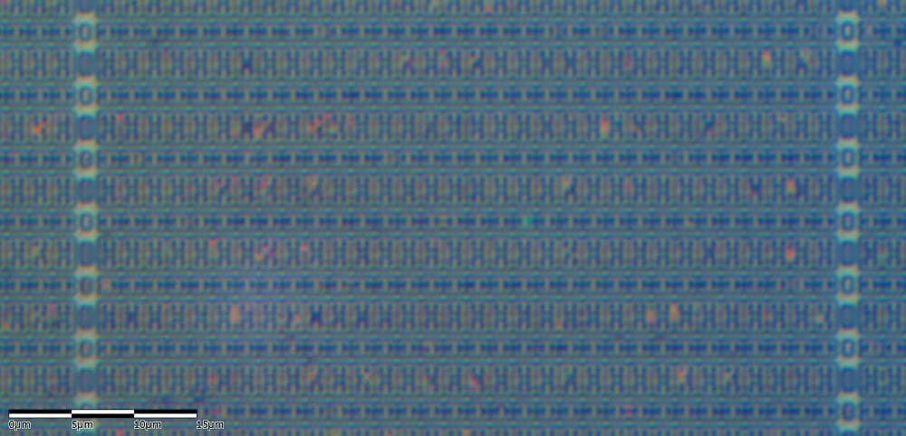
Cosa rappresenta ciascuno dei 4.096 bit

Il progetto incorporato mostra come un singolo bit di memoria statica si mantiene: un anello di due invertitori. La macro di questo gradino è costituita da 4.096 bit di memoria statica in un unico array.
3

I pin della macro e tre cose che il suo modello indica

gf180mcu_fd_ip_sram__sram512x8m8wm1 contiene 512 byte. I suoi pin: CLK; A, un indirizzo a 9 bit; D, il byte da scrivere; Q, il byte letto. I tre controlli sono tutti attivi LOW. CEN a 0 accende la memoria. GWEN a 0 fa sì che il fronte di clock sia una scrittura, a 1 una lettura. WEN ha un bit per ogni bit di dato, e uno 0 consente la scrittura di quel bit, quindi una scrittura può modificare alcuni bit di un byte lasciando invariati gli altri. Leggendo il modello di simulazione della PDK emergono tre aspetti utili. Primo, la memoria funziona solo dopo che CEN è passato da 1 a 0; altrimenti il modello stampa «CEN is not reset, memory is not operational», quindi il core mantiene CEN a 1 durante il reset e lo abbassa successivamente. Secondo, una lettura fornisce mem[A] su Q subito dopo il fronte di clock che ha campionato A, quindi i dati sono pronti un ciclo di clock dopo. Terzo, il modello parte con ogni byte a 0. Un chip reale non fa così: il suo SRAM all'accensione contiene il valore in cui è caduta ogni cella, quindi il progetto deve scrivere prima di leggere. L'esempio del template collega CEN a 1, quindi le sue due macro restano disattivate. I file di temporizzazione indicano il periodo minimo di clock della macro come 6.6 ns nell'angolo tipico a 5 V e 18.3 ns nell'angolo lento a 3.0 V, 125 °C, entrambi ampiamente entro i 40 ns del template.
4

The core

src/chip_core.sv for the pattern player, with the template's port list unchanged plus one parameter, HOLD_LOG2. Input pad 0 enables, pad 1 selects LOAD mode, pad 2 is the write strobe; bidirectional pads 0 to 7 carry the byte, pad 8 the PWM. The LOAD and strobe pads are passed through two flip-flops before use, a synchroniser: they change whenever the outside world likes, not in step with the chip's clock, and a flip-flop caught mid-change can hover between 0 and 1 for a while. In play mode, each time HOLD_LOG2 periods have passed, the byte the SRAM has been reading becomes the new duty and the address moves on.
chip_core.svsystemverilog
// SPDX-License-Identifier: Apache-2.0
// Youblob silicon rung 5: the PWM dimmer plays a brightness pattern stored in the on-chip SRAM macro.
// Port list unchanged from wafer-space/gf180mcu-project-template src/chip_core.sv.

`default_nettype none

module chip_core #(
    parameter NUM_INPUT_PADS,
    parameter NUM_BIDIR_PADS,
    parameter NUM_ANALOG_PADS,
    parameter HOLD_LOG2 = 9        // each table entry lasts 2**HOLD_LOG2 PWM periods
    )(
    `ifdef USE_POWER_PINS
    inout  wire VDD,
    inout  wire VSS,
    `endif

    input  wire clk,       // clock
    input  wire rst_n,     // reset (active low)

    input  wire [NUM_INPUT_PADS-1:0] input_in,   // Input value
    output wire [NUM_INPUT_PADS-1:0] input_pu,   // Pull-up
    output wire [NUM_INPUT_PADS-1:0] input_pd,   // Pull-down

    input  wire [NUM_BIDIR_PADS-1:0] bidir_in,   // Input value
    output wire [NUM_BIDIR_PADS-1:0] bidir_out,  // Output value
    output wire [NUM_BIDIR_PADS-1:0] bidir_oe,   // Output enable
    output wire [NUM_BIDIR_PADS-1:0] bidir_cs,   // Input type (0=CMOS Buffer, 1=Schmitt Trigger)
    output wire [NUM_BIDIR_PADS-1:0] bidir_sl,   // Slew rate (0=fast, 1=slow)
    output wire [NUM_BIDIR_PADS-1:0] bidir_ie,   // Input enable
    output wire [NUM_BIDIR_PADS-1:0] bidir_pu,   // Pull-up
    output wire [NUM_BIDIR_PADS-1:0] bidir_pd,   // Pull-down

    inout  wire [NUM_ANALOG_PADS-1:0] analog  // Analog
);

    // Input pad 0: enable.  Input pad 1: LOAD mode.  Input pad 2: write strobe.
    // Bidir pads 0..7: the byte to store while loading.  Bidir pad 8: the PWM output.
    localparam DUTY_W = 8;
    localparam PWM_PAD = 8;

    assign input_pu = '0;
    assign input_pd = '0;
    assign bidir_oe = {{(NUM_BIDIR_PADS-DUTY_W){1'b1}}, {DUTY_W{1'b0}}};
    assign bidir_ie = ~bidir_oe;
    assign bidir_cs = {{(NUM_BIDIR_PADS-DUTY_W){1'b0}}, {DUTY_W{1'b1}}};
    assign bidir_sl = '0;
    assign bidir_pu = '0;
    assign bidir_pd = '0;

    wire enable = input_in[0];
    wire [DUTY_W-1:0] data_in = bidir_in[DUTY_W-1:0];

    // The mode and strobe pads change whenever the outside world likes, not in step with clk:
    // two flip-flops in a row (a synchroniser) before anything uses them.
    logic [1:0] load_s;
    logic [2:0] strobe_s;
    always_ff @(posedge clk) begin
        load_s   <= {load_s[0], input_in[1]};
        strobe_s <= {strobe_s[1:0], input_in[2]};
    end
    logic load_was;
    wire load        = load_s[1];
    wire load_start  = load & ~load_was;
    wire strobe_rise = strobe_s[1] & ~strobe_s[2];
    always_ff @(posedge clk) load_was <= load;

    // The SRAM wants its chip enable (CEN, active LOW) to go 1 -> 0 before it works:
    // hold it at 1 through reset, then 0.
    logic cen;
    always_ff @(posedge clk) cen <= !rst_n;

    // PWM counter and the "hold" counter that decides when to step to the next table entry.
    logic [DUTY_W-1:0] count;
    logic [HOLD_LOG2:0] hold;                   // one bit wider so HOLD_LOG2 = 0 still works
    wire period_end = (count == '1);
    localparam logic [HOLD_LOG2:0] HOLD_MASK = (1 << HOLD_LOG2) - 1;   // 0 when HOLD_LOG2 = 0
    wire step = period_end && ((hold & HOLD_MASK) == HOLD_MASK);

    logic [DUTY_W-1:0] addr;
    logic [DUTY_W-1:0] duty;
    wire  [DUTY_W-1:0] q;                       // SRAM read data: mem[addr], one clock after addr

    always_ff @(posedge clk) begin
        if (!rst_n) begin
            count <= '0;  hold <= '0;  addr <= '0;  duty <= '0;
        end else if (load) begin
            count <= '0;  hold <= '0;  duty <= '0;
            if (load_start)       addr <= '0;       // every load starts at entry 0
            else if (strobe_rise) addr <= addr + 1'b1;
        end else if (enable) begin
            count <= count + 1'b1;
            if (period_end) hold <= hold + 1'b1;
            if (step) begin
                duty <= q;                          // the entry that was being read
                addr <= addr + 1'b1;                // and move on to the next
            end
        end
    end

    `gf180mcu_xxx_ip_sram__sram512x8m8wm1 sram_0 (
        `ifdef USE_POWER_PINS
        .VDD  (VDD),
        .VSS  (VSS),
        `endif
        .CLK  (clk),
        .CEN  (cen),                                   // active low: 0 = on
        .GWEN (~(load && strobe_rise)),                // active low: 0 = write this clock
        .WEN  (8'b0),                                  // active low, per bit: write all eight
        .A    ({1'b0, addr}),                          // 256 of the 512 bytes
        .D    (data_in),
        .Q    (q)
    );

    logic pwm;
    always_ff @(posedge clk) begin
        if (!rst_n) pwm <= 1'b0;
        else        pwm <= enable && !load && (count < duty);
    end

    logic [NUM_BIDIR_PADS-1:0] out;
    always_comb begin
        out = '0;
        out[PWM_PAD] = pwm;
    end
    assign bidir_out = out;

    // Inputs this design does not read (keeps lint quiet, as the template does with _unused).
    logic _unused;
    assign _unused = &{1'b0, input_in[NUM_INPUT_PADS-1:3], bidir_in[NUM_BIDIR_PADS-1:DUTY_W], hold[HOLD_LOG2]};

endmodule

`default_nettype wire

Strumenti necessari:

Computer da tavoloComputer da tavolo
5

The test

test_pattern.py builds the core with the PDK's SRAM model, gf180mcu_fd_ip_sram__sram512x8m8wm1.v, at the template's 25 MHz and with HOLD_LOG2 = 0 so the whole table plays in 256 periods. It loads the table through the pads the way the ESP32 will, then counts the high clocks in each of 600 PWM periods and requires them to follow the table from exactly one starting point. A second test loads again and checks the new pattern replaced the old.
test_pattern.pypython
# SPDX-License-Identifier: Apache-2.0
# cocotb testbench for the SRAM pattern player, with the PDK's own SRAM simulation model
# (gf180mcu_fd_ip_sram__sram512x8m8wm1, gf180mcuD, the commit the template pins).
import math
import os
from pathlib import Path

import cocotb
from cocotb.clock import Clock
from cocotb.triggers import ClockCycles, FallingEdge, RisingEdge
from cocotb_tools.runner import get_runner

PWM_PAD = 8
EN, LOAD, STROBE = 1, 2, 4                      # input pad bits
SRAM = Path(os.getenv("PDK_ROOT", "pdk")) / "gf180mcuD" / "libs.ref" / "gf180mcu_fd_ip_sram" / "verilog"


def breathing_table(n=256, gamma=2.2):
    """One slow breath: a raised sine, gamma-corrected so equal steps LOOK equal to the eye."""
    return [round(255 * ((1 - math.cos(2 * math.pi * i / n)) / 2) ** gamma) for i in range(n)]


async def start(dut):
    cocotb.start_soon(Clock(dut.clk, 40, unit="ns").start())   # 25 MHz, the template's CLOCK_PERIOD
    dut.input_in.value = 0
    dut.bidir_in.value = 0
    dut.rst_n.value = 0
    await ClockCycles(dut.clk, 5)
    dut.rst_n.value = 1
    await ClockCycles(dut.clk, 2)


async def load(dut, table):
    """What a microcontroller on the breakout does: LOAD high, then per byte set the data pads,
    raise the strobe, wait, lower it. The chip synchronises the strobe, so hold each for 4 clocks."""
    dut.input_in.value = LOAD
    await ClockCycles(dut.clk, 4)
    for b in table:
        dut.bidir_in.value = b
        await ClockCycles(dut.clk, 1)
        dut.input_in.value = LOAD | STROBE
        await ClockCycles(dut.clk, 4)
        dut.input_in.value = LOAD
        await ClockCycles(dut.clk, 4)
    dut.input_in.value = 0
    await ClockCycles(dut.clk, 4)


async def highs_per_period(dut, periods):
    """High clocks in each PWM period, counted from the core's own count = 0."""
    while int(dut.count.value) != 0:
        await RisingEdge(dut.clk)
    out = []
    for _ in range(periods):
        n = 0
        for _ in range(256):
            await FallingEdge(dut.clk)
            n += int(dut.bidir_out.value[PWM_PAD])
        out.append(n)
    return out


@cocotb.test()
async def test_plays_the_table(dut):
    """Load a 256-entry breathing table, play it: each period's high time is the next entry."""
    table = breathing_table()
    await start(dut)
    await load(dut, table)
    dut.input_in.value = EN
    got = await highs_per_period(dut, 600)
    # the output starts part-way through the table; find where, then demand every period match
    fits = [off for off in range(256) if all(got[j] == table[(j + off) % 256] for j in range(2, 600))]
    dut._log.info(f"first periods {got[:8]}, table aligns at offset {fits}")
    Path(__file__).resolve().parent.joinpath("pattern_trace.csv").write_text("\n".join(map(str, got)))
    assert len(fits) == 1, f"the output does not follow the table (offsets that fit: {fits})"


@cocotb.test()
async def test_reload(dut):
    """Loading again replaces the pattern: a flat 64 gives 64 high clocks every period."""
    await start(dut)
    await load(dut, breathing_table())
    await load(dut, [64] * 256)
    dut.input_in.value = EN
    got = await highs_per_period(dut, 40)
    assert all(g == 64 for g in got[2:]), got


def test_runner():
    here = Path(__file__).resolve().parent
    defines = {"gf180mcu_xxx_ip_sram__sram512x8m8wm1": "gf180mcu_fd_ip_sram__sram512x8m8wm1"}
    runner = get_runner("icarus")
    runner.build(
        sources=[SRAM / "gf180mcu_fd_ip_sram__sram512x8m8wm1.v", here / "chip_core.sv"],
        hdl_toplevel="chip_core",
        parameters={"NUM_INPUT_PADS": 4, "NUM_BIDIR_PADS": 38, "NUM_ANALOG_PADS": 4, "HOLD_LOG2": 0},
        defines=defines,
        build_args=["-g2012"],
        timescale=("1ns", "1ps"),
        always=True,
    )
    runner.test(hdl_toplevel="chip_core", test_module="test_pattern")


if __name__ == "__main__":
    test_runner()

Strumenti necessari:

Computer da tavoloComputer da tavolo
6

Cosa ha stampato la simulazione

Esecuzione di questo blueprint con Icarus Verilog 12.0 e cocotb 2.1.0: -------- MESSAGE: CEN appena resettato, la memoria è operativa --------- test_pattern.test_plays_the_table PASS (600 periodi, la tabella si allinea a esattamente un offset) test_pattern.test_reload PASS TESTS=2 PASS=2 FAIL=0 SKIP=0 Per dimostrare che il test può fallire, WEN è stato cambiato da 8'b0 a 8'hFF, il classico errore con un pin attivo basso: ogni bit mascherato, nulla scritto, una tabella di zeri. Entrambi i test sono falliti e il core è stato ripristinato. La prima riga è il messaggio del modello SRAM: il core ha abbassato CEN dopo il reset, come richiede il modello.
7

Load it from an ESP32

Once the chip is on its breakout board, this sketch writes the table. Eight GPIOs carry the byte, three more drive LOAD, the strobe and enable, and an LED with a 330 ohm resistor from pad 8 to ground shows the breath. Each level is held for 1 microsecond, 25 of the chip's clocks, so the synchroniser always sees it. The sketch then does nothing: the pattern lives in the chip. It is lost when the chip loses power, so send r over serial to load it again. The ESP32 is a 3.3 V part and its inputs are not 5 V tolerant. The sketch only drives the chip and never reads from it. The template's default libraries are the 5 V ones; before you connect, check in the I/O library's documentation that 3.3 V is a valid logic high for your chip's inputs, or build with the 3.3 V libraries, as the template's README shows. The sketch compiles for the ESP32 with the Arduino ESP32 core 3.3.12; it has not been run, because the chip does not exist yet.
load_pattern.inocpp
// SPDX-License-Identifier: Apache-2.0
// Load a breathing pattern into your chip's SRAM through its pads, then let the chip play it.
// Youblob silicon rung 5. The chip does the playing; this board only writes 256 bytes once.
//
// Wiring (ESP32 GPIO -> chip pad on your breakout):
//   D0..D7  GPIO 13,14,18,19,21,22,23,25 -> bidir[0..7]
//   LOAD    GPIO 26 -> input[1]
//   STROBE  GPIO 27 -> input[2]
//   EN      GPIO 32 -> input[0]
//   and a common ground. The chip's bidir[8] drives an LED through 330 ohm to ground.
// The ESP32 is a 3.3 V part: run the chip's I/O at 3.3 V, or put a level shifter between them.

#include <math.h>

const int DATA_PINS[8] = {13, 14, 18, 19, 21, 22, 23, 25};
const int PIN_LOAD = 26, PIN_STROBE = 27, PIN_EN = 32;

// The chip passes LOAD and STROBE through a two-flip-flop synchroniser and looks for the strobe's
// rising edge, so every level has to last a few of ITS clocks. 1 us is 25 clocks at 25 MHz.
const unsigned HOLD_US = 1;

uint8_t table[256];

void makeBreathingTable() {
  // a raised sine, gamma-corrected (2.2) so the brightness steps look even to the eye
  for (int i = 0; i < 256; i++) {
    float s = (1.0f - cosf(2.0f * PI * i / 256.0f)) / 2.0f;
    table[i] = (uint8_t)lroundf(255.0f * powf(s, 2.2f));
  }
}

void putByte(uint8_t b) {
  for (int bit = 0; bit < 8; bit++) digitalWrite(DATA_PINS[bit], (b >> bit) & 1);
  delayMicroseconds(HOLD_US);            // data settles before the strobe
  digitalWrite(PIN_STROBE, HIGH);        // the chip writes on the strobe's rising edge...
  delayMicroseconds(HOLD_US);            // ...a few of its clocks later, so hold the data
  digitalWrite(PIN_STROBE, LOW);
  delayMicroseconds(HOLD_US);
}

void loadTable() {
  digitalWrite(PIN_EN, LOW);
  digitalWrite(PIN_LOAD, HIGH);          // entering LOAD resets the chip's address to 0
  delayMicroseconds(HOLD_US);
  for (int i = 0; i < 256; i++) putByte(table[i]);
  digitalWrite(PIN_LOAD, LOW);
  delayMicroseconds(HOLD_US);
}

void setup() {
  Serial.begin(115200);
  for (int bit = 0; bit < 8; bit++) pinMode(DATA_PINS[bit], OUTPUT);
  pinMode(PIN_LOAD, OUTPUT);
  pinMode(PIN_STROBE, OUTPUT);
  pinMode(PIN_EN, OUTPUT);
  digitalWrite(PIN_STROBE, LOW);

  makeBreathingTable();
  loadTable();
  digitalWrite(PIN_EN, HIGH);            // play
  Serial.println("pattern loaded; the chip is playing it on its own");
  Serial.printf("table[0]=%u table[64]=%u table[128]=%u\n", table[0], table[64], table[128]);
}

void loop() {
  // Nothing to do: the pattern lives in the chip's SRAM now.
  // Send 'r' over serial to load it again (the SRAM loses it when the chip loses power).
  if (Serial.available() && Serial.read() == 'r') {
    loadTable();
    digitalWrite(PIN_EN, HIGH);
    Serial.println("reloaded");
  }
}

Materiali per questo passaggio:

Chip ASIC personalizzatoChip ASIC personalizzato1 pezzo
Circuito stampatoCircuito stampato1 pezzo
LED da 5 mmLED da 5 mm1 pezzo
Resistenza da 330 ohmResistenza da 330 ohm1 pezzo

Strumenti necessari:

Scheda di sviluppo ESP32Scheda di sviluppo ESP32
BreadboardBreadboard
Cavetti ponticelloCavetti ponticello
Computer da tavoloComputer da tavolo
8

Un pattern che non si salva o non riproduce

Risoluzione dei problemi del pattern SRAM.

Flow

Loading...
9

Fonti e limiti onesti

**Fonti**, consultate il 29 settembre 2026: il GF180MCU PDK al commit fissato dal template (gf180mcuD, f6eeac7dad085ffcc829ccfd721f7b4ce39edcf7, dalle release fossi-foundation ciel; Apache-2.0): il modello SRAM gf180mcu_fd_ip_sram__sram512x8m8wm1.v, il suo LEF per il contorno e i file di timing per il periodo minimo di clock; il file di timing della libreria di celle standard per l'area dei flip-flop. Il repository wafer-space/gf180mcu-project-template (src/chip_core.sv, src/chip_top.sv, README.md, librelane/config.yaml; Apache-2.0). **Limiti onesti.** La simulazione è a livello chip_core, con il modello proprio del SRAM ma senza il pad ring, la sintesi o il layout, e i controlli di timing del modello non decidono nulla qui. Lo sketch ESP32 è stato compilato, non eseguito. HOLD_LOG2 era 0 nel test così che terminasse; il chip userebbe 9, un respiro di circa 1,3 s.

Materiali

4

Strumenti richiesti

4

CC0 Pubblico dominio

Questo progetto è rilasciato sotto CC0. Sei libero di copiare, modificare, distribuire e utilizzare quest'opera per qualsiasi scopo, senza chiedere permesso.

Supporta il Maker acquistando prodotti tramite il suo progetto dove guadagna una Commissione Maker stabilita dai venditori, oppure crea una nuova iterazione di questo progetto e includilo come collegamento nel tuo progetto per condividere i ricavi.

Commenti

(0)

Accedi per partecipare alla discussione

Caricamento commenti...