アート
美容とウェルネス
工芸
文化と歴史
エンターテインメント
環境
食品と飲料
グリーンフューチャー
リバースエンジニアリング
科学
スポーツ
テクノロジー
ウェアラブル
Understanding Indium from Zinc Ore — The Soft Metal Behind Every Touchscreen
中級者
手順
1
1
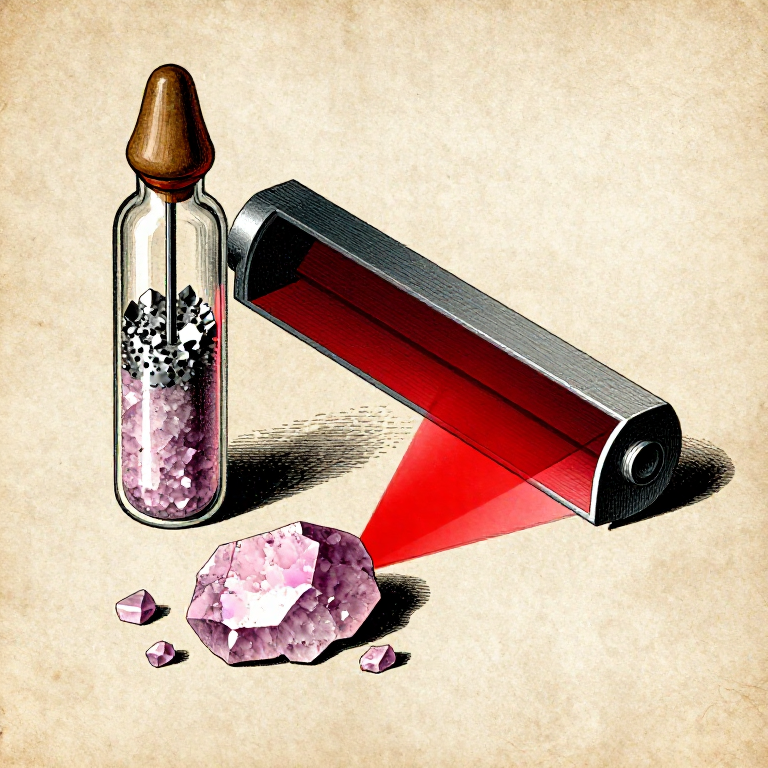
Understand Indium's Spectroscopic Discovery
Understand Indium's Spectroscopic Discovery
Ferdinand Reich and Hieronymus Theodor Richter discovered indium in 1863 at the Freiberg School of Mines while spectroscopically analyzing zinc blende (sphalerite) for thallium. They found a brilliant indigo-blue spectral line never seen before — hence 'indium' from the Latin 'indicium' (indigo). Reich was color-blind and could not see the line himself; his assistant Richter confirmed the color. The discovery required only a spectroscope and a zinc ore sample.
2
2
Identify Indium Sources
Identify Indium Sources
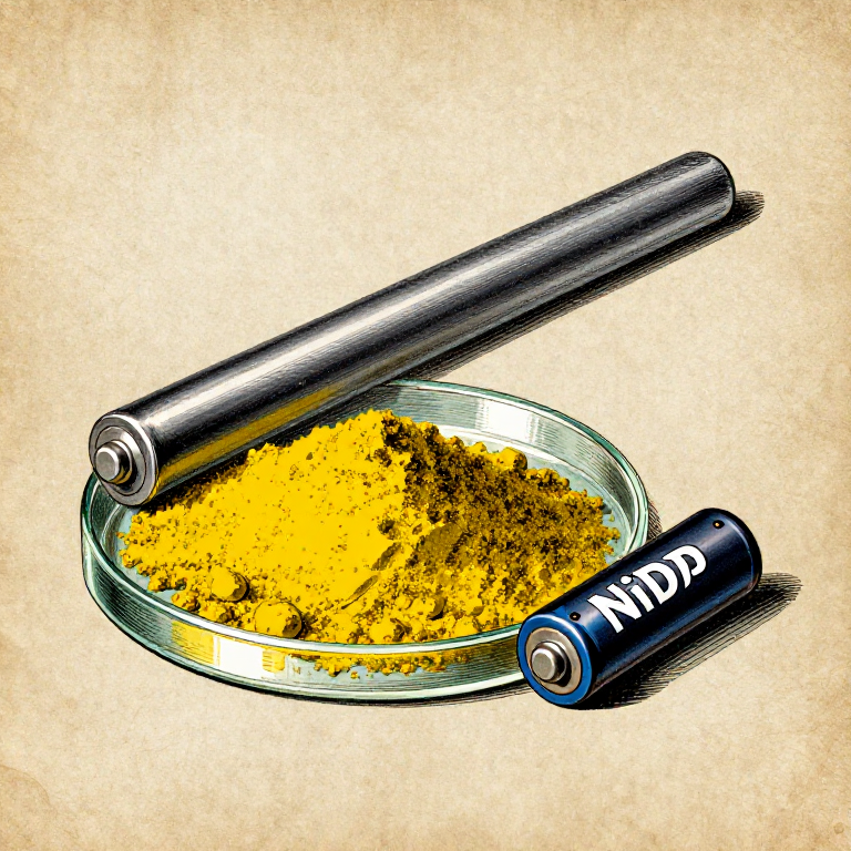
Indium has no ore of its own — it occurs at 10-20 ppm in sphalerite (zinc sulfide), substituting for zinc in the crystal lattice. All commercial indium is recovered as a byproduct of zinc refining. China produces 50% of global supply (approximately 900 tonnes annually), followed by South Korea and Japan. The total identified global resource is only about 50,000 tonnes, making indium one of the scarcest technology metals.
このステップの材料:
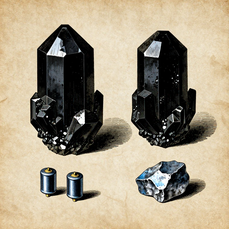
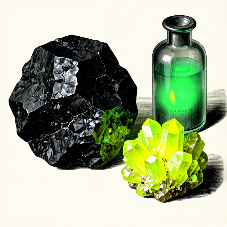
 Sphalerite Ore (zinc sulfide)
必要な工具:
Hand Lens (10x Magnification)
3
3
Trace the Zinc Refinery Recovery Process
Trace the Zinc Refinery Recovery Process
During electrolytic zinc refining, indium accumulates in the residues and anode slimes. The residue is leached with hydrochloric acid, and indium is selectively extracted by solvent extraction using di(2-ethylhexyl)phosphoric acid (D2EHPA). Cementation on aluminum strips from acid solution is a simpler alternative. Final purification to 99.999% (5N) grade uses zone refining or electrolytic refining in indium sulfamate baths.
このステップの材料:
Sphalerite Ore (zinc sulfide)必要な工具:
 Safety Goggles
 Chemical-Resistant Gloves
4
4
Examine Indium Metal Properties
Examine Indium Metal Properties
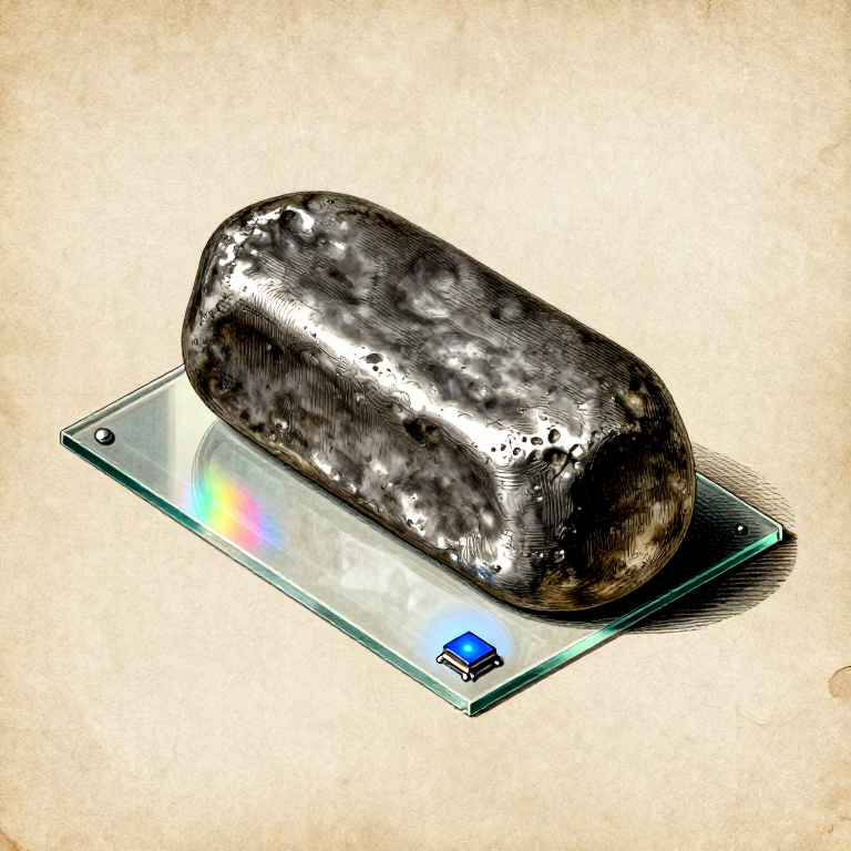
Indium is remarkably soft — softer than lead — and leaves a visible streak on paper. It emits a high-pitched 'tin cry' when bent as crystal planes shear. Melting point is 156.6°C, density 7.31 g/cm³. Indium wets glass, making it useful as a sealant for glass-to-metal joints in vacuum systems. It remains ductile and malleable down to cryogenic temperatures, unlike most metals that become brittle. Indium metal is non-toxic.
5
5
Understand Indium Tin Oxide Technology
Understand Indium Tin Oxide Technology
Indium tin oxide (ITO) — 90% In₂O₃, 10% SnO₂ — is a transparent electrical conductor, the only material that combines high optical transparency (>85% in visible spectrum) with low electrical resistivity. Every touchscreen on every smartphone, tablet, and laptop uses an ITO coating sputtered onto glass. The coating is just 100-200 nanometers thick — invisible to the eye but conducting enough to sense finger position. ITO consumes 65% of global indium production.
6
6
Explore LED and Semiconductor Applications
Explore LED and Semiconductor Applications
Indium gallium nitride (InGaN) is the active material in blue and white LEDs — every white LED lamp, phone screen backlight, and traffic signal uses this compound. Adjusting the indium-to-gallium ratio tunes emission from ultraviolet through blue to green. Indium phosphide (InP) is the substrate for high-speed fiber optic lasers and photodetectors operating at 1.3 and 1.55 micrometer wavelengths — the standard for telecommunications.
7
7
Discover Soldering and Thermal Interface Uses
Discover Soldering and Thermal Interface Uses
Indium-based solders (In-Sn, In-Ag, In-Bi) melt at temperatures as low as 118°C, enabling assembly of heat-sensitive components. Pure indium thermal interface material (TIM) between a CPU and its heatsink provides superior heat transfer because indium's softness allows it to conform perfectly to microscopic surface roughness. Indium foil seals in cryogenic equipment because it remains ductile at liquid helium temperature (4 K).
8
8
Survey CIGS Solar Cell Technology
Survey CIGS Solar Cell Technology
Copper indium gallium selenide (CIGS) thin-film solar cells achieve 23.6% laboratory efficiency — the highest of any thin-film technology. The CIGS absorber layer is only 1-2 micrometers thick, using 100 times less semiconductor material than silicon wafers. CIGS panels can be deposited on flexible substrates for building-integrated photovoltaics. However, indium scarcity limits CIGS to niche applications compared to silicon and cadmium telluride.
9
9
Assess Supply Chain Vulnerability
Assess Supply Chain Vulnerability
Indium faces unique supply risks: production depends entirely on zinc mining decisions (no dedicated indium mines), recycling rates are below 1% (most indium in touchscreens and LEDs is too dispersed to recover), and demand is growing 5-10% annually as touchscreen and LED adoption expands globally. In 2023, China restricted indium exports alongside gallium and germanium, highlighting semiconductor supply chain fragility.
必要な工具:
 Precision Scale (0.01g)
10
10
Document Findings and Substitution Challenges
Document Findings and Substitution Challenges
Record indium's key data: atomic number 49, density 7.31 g/cm³, melting point 156.6°C, very soft silvery metal. Replacing ITO is one of the most active research areas in materials science — candidates include graphene, silver nanowires, carbon nanotubes, and PEDOT:PSS conducting polymer. None yet match ITO's combination of transparency, conductivity, processability, and durability. Until a replacement scales commercially, indium remains indispensable for the display industry.
必要な工具
4- プレースホルダー
- プレースホルダー
- プレースホルダー
接続ブループリントの材料
Related blueprints
Other builds that share materials, tools, or techniques with this one.
Understanding Tantalum from Columbite-Tantalite — The Conflict Metal Inside Every Phonechemistry
Understanding Cadmium from Zinc Smelting — The Toxic Metal in Rechargeable Batterieschemistry
Understanding Beryllium from Beryl — The Toxic Gem Metal Behind Emeraldschemistry
Understanding Uranium from Uraninite — The Element That Changed Everythingchemistry
Understanding Zirconium from Zircon — The Ancient Gemstone That Clocks Earth's Agechemistry
Understanding Rubidium from Lepidolite — The Alkali Metal That Defines Timechemistry
CC0 パブリックドメイン
このブループリントはCC0で公開されています。許可を求めずに、自由にコピー、修正、配布、あらゆる目的で使用できます。
メイカーを応援するには、ブループリント経由で製品を購入してください。メイカーには メイカーコミッション がベンダーにより設定されています。または、このブループリントの新しいイテレーションを作成し、自分のブループリントにコネクションとして含めて収益を共有できます。