Ushirikiano
SANAA
UREMBO NA USTAWI
UJANJA
UTAMADUNI NA HISTORIA
BURUDANI
MAZINGIRA
CHAKULA NA VINYWAJI
UHANDISI WA KINYUME
SAYANSI
MICHEZO
TEKNOLOJIA
VAZI
Kumbukumbu ya SRAM Ndani ya Chip: Mwanga Unaopumua Uliohifadhiwa Kwenye Kumbukumbu ya Chip Yako
English
Youblob (simulation output) · CC0
Ed

Imeundwa na

Ed

29. Septemba 2026FI
51
0
0
0
0

Kumbukumbu ya SRAM Ndani ya Chip: Mwanga Unaopumua Uliohifadhiwa Kwenye Kumbukumbu ya Chip Yako

Kiolezo cha wafer.space kinakuja na macros mbili za SRAM katika muundo wake wa mfano, kila moja ikiwa na baiti 512, na zimezimwa. Macro ni kizuizi kilichokamilika cha kumbukumbu kutoka PDK: seli 4,096 za kumbukumbu tuli, zilizochorwa mara moja pamoja na kisimbuaji cha anwani na saketi za kusoma, unazoweka zote kwa pamoja badala ya kuzijenga kutoka kwenye gates. Hatua hii inawasha moja kati yake. Dimmer ya PWM kutoka hatua iliyotangulia sasa inacheza mfuatano: microcontroller inaandika baiti 256 kwenye chip kupitia pads zake, mara moja, na kuanzia hapo chip inazisoma yenyewe, baiti moja kwa hatua, kama mwangaza wa taa inayopumua polepole. Core na testbench yake viliendeshwa kwa blueprint hii kwa kutumia Icarus Verilog 12.0, cocotb 2.1.0 na modeli ya simulation ya PDK yenyewe ya macro ya SRAM: matokeo yalifuata jedwali lililohifadhiwa kwa vipindi 600 vya PWM. Picha ni matokeo ya simulation hiyo yenyewe, upau mmoja kwa kila kipindi. Mchoro wa ESP32 unaopakia jedwali ulikusanywa kwa blueprint hii; bado hakuna chip ya kuuendesha.
Juu
Jioni, pamoja na chip

Maagizo

1

Muundo, muda na ukubwa

Inapakia daftari la Jupyter…
2

Kila moja ya biti 4,096 ni nini

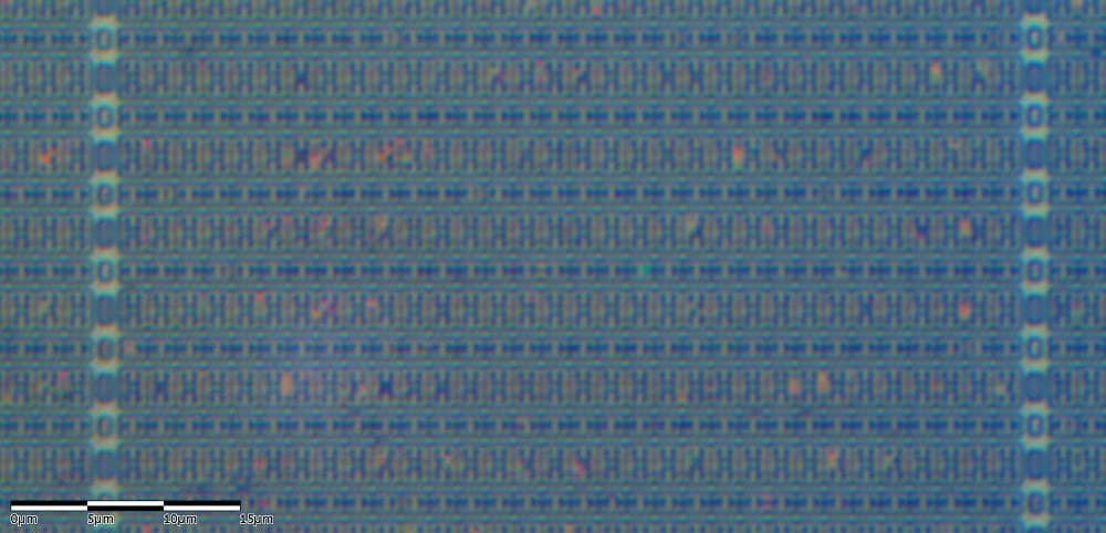
Mchoro uliopachikwa unaonyesha jinsi biti moja ya kumbukumbu tuli inavyojishikilia yenyewe: kitanzi cha vibadilishi viwili (inverters). Macro katika ngazi hii ni biti 4,096 za kumbukumbu tuli katika safu moja.
3

Pini za macro, na mambo matatu ambayo modeli yake inasema

gf180mcu_fd_ip_sram__sram512x8m8wm1 inashikilia baiti 512. Pini zake: CLK; A, anwani ya biti 9; D, baiti ya kuandika; Q, baiti iliyosomwa. Vidhibiti vitatu vyote ni vinavyofanya kazi kwa kiwango cha LOW. CEN ikiwa 0 huwasha kumbukumbu. GWEN ikiwa 0 hufanya ukingo wa saa kuwa uandishi, ikiwa 1 ni usomaji. WEN ni biti moja kwa kila biti ya data, na 0 huruhusu biti hiyo kuandikwa, hivyo uandishi unaweza kubadilisha baadhi ya biti za baiti na kuacha nyingine bila kuguswa. Kusoma modeli ya uigaji ya PDK kunaonyesha mambo matatu yanayostahili kujulikana. Kwanza, kumbukumbu hufanya kazi tu baada ya CEN kubadilika kutoka 1 hadi 0; vinginevyo modeli huchapisha "CEN is not reset, memory is not operational", hivyo core inashikilia CEN kuwa 1 wakati wa reset na kuishusha baadaye. Pili, usomaji hutoa mem[A] kwenye Q mara baada ya ukingo wa saa uliosampuli A, hivyo data iko tayari saa moja baadaye. Tatu, modeli huanza na kila baiti ikiwa 0. Chip halisi haifanyi hivyo: SRAM yake huwashwa ikiwa na chochote kila seli ilichoanguka nacho, hivyo muundo lazima uandike kabla ya kusoma. Mfano wa template yenyewe unafunga CEN kuwa 1, hivyo macro zake mbili zimezimwa. Faili zake za muda zinaonyesha kipindi cha chini cha saa cha macro kuwa 6.6 ns katika kona ya kawaida ya 5 V na 18.3 ns katika kona ya polepole ya 3.0 V, 125 °C, zote mbili zikiwa ndani ya 40 ns ya template.
4

The core

src/chip_core.sv for the pattern player, with the template's port list unchanged plus one parameter, HOLD_LOG2. Input pad 0 enables, pad 1 selects LOAD mode, pad 2 is the write strobe; bidirectional pads 0 to 7 carry the byte, pad 8 the PWM. The LOAD and strobe pads are passed through two flip-flops before use, a synchroniser: they change whenever the outside world likes, not in step with the chip's clock, and a flip-flop caught mid-change can hover between 0 and 1 for a while. In play mode, each time HOLD_LOG2 periods have passed, the byte the SRAM has been reading becomes the new duty and the address moves on.
chip_core.svsystemverilog
// SPDX-License-Identifier: Apache-2.0
// Youblob silicon rung 5: the PWM dimmer plays a brightness pattern stored in the on-chip SRAM macro.
// Port list unchanged from wafer-space/gf180mcu-project-template src/chip_core.sv.

`default_nettype none

module chip_core #(
    parameter NUM_INPUT_PADS,
    parameter NUM_BIDIR_PADS,
    parameter NUM_ANALOG_PADS,
    parameter HOLD_LOG2 = 9        // each table entry lasts 2**HOLD_LOG2 PWM periods
    )(
    `ifdef USE_POWER_PINS
    inout  wire VDD,
    inout  wire VSS,
    `endif

    input  wire clk,       // clock
    input  wire rst_n,     // reset (active low)

    input  wire [NUM_INPUT_PADS-1:0] input_in,   // Input value
    output wire [NUM_INPUT_PADS-1:0] input_pu,   // Pull-up
    output wire [NUM_INPUT_PADS-1:0] input_pd,   // Pull-down

    input  wire [NUM_BIDIR_PADS-1:0] bidir_in,   // Input value
    output wire [NUM_BIDIR_PADS-1:0] bidir_out,  // Output value
    output wire [NUM_BIDIR_PADS-1:0] bidir_oe,   // Output enable
    output wire [NUM_BIDIR_PADS-1:0] bidir_cs,   // Input type (0=CMOS Buffer, 1=Schmitt Trigger)
    output wire [NUM_BIDIR_PADS-1:0] bidir_sl,   // Slew rate (0=fast, 1=slow)
    output wire [NUM_BIDIR_PADS-1:0] bidir_ie,   // Input enable
    output wire [NUM_BIDIR_PADS-1:0] bidir_pu,   // Pull-up
    output wire [NUM_BIDIR_PADS-1:0] bidir_pd,   // Pull-down

    inout  wire [NUM_ANALOG_PADS-1:0] analog  // Analog
);

    // Input pad 0: enable.  Input pad 1: LOAD mode.  Input pad 2: write strobe.
    // Bidir pads 0..7: the byte to store while loading.  Bidir pad 8: the PWM output.
    localparam DUTY_W = 8;
    localparam PWM_PAD = 8;

    assign input_pu = '0;
    assign input_pd = '0;
    assign bidir_oe = {{(NUM_BIDIR_PADS-DUTY_W){1'b1}}, {DUTY_W{1'b0}}};
    assign bidir_ie = ~bidir_oe;
    assign bidir_cs = {{(NUM_BIDIR_PADS-DUTY_W){1'b0}}, {DUTY_W{1'b1}}};
    assign bidir_sl = '0;
    assign bidir_pu = '0;
    assign bidir_pd = '0;

    wire enable = input_in[0];
    wire [DUTY_W-1:0] data_in = bidir_in[DUTY_W-1:0];

    // The mode and strobe pads change whenever the outside world likes, not in step with clk:
    // two flip-flops in a row (a synchroniser) before anything uses them.
    logic [1:0] load_s;
    logic [2:0] strobe_s;
    always_ff @(posedge clk) begin
        load_s   <= {load_s[0], input_in[1]};
        strobe_s <= {strobe_s[1:0], input_in[2]};
    end
    logic load_was;
    wire load        = load_s[1];
    wire load_start  = load & ~load_was;
    wire strobe_rise = strobe_s[1] & ~strobe_s[2];
    always_ff @(posedge clk) load_was <= load;

    // The SRAM wants its chip enable (CEN, active LOW) to go 1 -> 0 before it works:
    // hold it at 1 through reset, then 0.
    logic cen;
    always_ff @(posedge clk) cen <= !rst_n;

    // PWM counter and the "hold" counter that decides when to step to the next table entry.
    logic [DUTY_W-1:0] count;
    logic [HOLD_LOG2:0] hold;                   // one bit wider so HOLD_LOG2 = 0 still works
    wire period_end = (count == '1);
    localparam logic [HOLD_LOG2:0] HOLD_MASK = (1 << HOLD_LOG2) - 1;   // 0 when HOLD_LOG2 = 0
    wire step = period_end && ((hold & HOLD_MASK) == HOLD_MASK);

    logic [DUTY_W-1:0] addr;
    logic [DUTY_W-1:0] duty;
    wire  [DUTY_W-1:0] q;                       // SRAM read data: mem[addr], one clock after addr

    always_ff @(posedge clk) begin
        if (!rst_n) begin
            count <= '0;  hold <= '0;  addr <= '0;  duty <= '0;
        end else if (load) begin
            count <= '0;  hold <= '0;  duty <= '0;
            if (load_start)       addr <= '0;       // every load starts at entry 0
            else if (strobe_rise) addr <= addr + 1'b1;
        end else if (enable) begin
            count <= count + 1'b1;
            if (period_end) hold <= hold + 1'b1;
            if (step) begin
                duty <= q;                          // the entry that was being read
                addr <= addr + 1'b1;                // and move on to the next
            end
        end
    end

    `gf180mcu_xxx_ip_sram__sram512x8m8wm1 sram_0 (
        `ifdef USE_POWER_PINS
        .VDD  (VDD),
        .VSS  (VSS),
        `endif
        .CLK  (clk),
        .CEN  (cen),                                   // active low: 0 = on
        .GWEN (~(load && strobe_rise)),                // active low: 0 = write this clock
        .WEN  (8'b0),                                  // active low, per bit: write all eight
        .A    ({1'b0, addr}),                          // 256 of the 512 bytes
        .D    (data_in),
        .Q    (q)
    );

    logic pwm;
    always_ff @(posedge clk) begin
        if (!rst_n) pwm <= 1'b0;
        else        pwm <= enable && !load && (count < duty);
    end

    logic [NUM_BIDIR_PADS-1:0] out;
    always_comb begin
        out = '0;
        out[PWM_PAD] = pwm;
    end
    assign bidir_out = out;

    // Inputs this design does not read (keeps lint quiet, as the template does with _unused).
    logic _unused;
    assign _unused = &{1'b0, input_in[NUM_INPUT_PADS-1:3], bidir_in[NUM_BIDIR_PADS-1:DUTY_W], hold[HOLD_LOG2]};

endmodule

`default_nettype wire

Zana zinazohitajika:

Kompyuta ya mezaniKompyuta ya mezani
5

The test

test_pattern.py builds the core with the PDK's SRAM model, gf180mcu_fd_ip_sram__sram512x8m8wm1.v, at the template's 25 MHz and with HOLD_LOG2 = 0 so the whole table plays in 256 periods. It loads the table through the pads the way the ESP32 will, then counts the high clocks in each of 600 PWM periods and requires them to follow the table from exactly one starting point. A second test loads again and checks the new pattern replaced the old.
test_pattern.pypython
# SPDX-License-Identifier: Apache-2.0
# cocotb testbench for the SRAM pattern player, with the PDK's own SRAM simulation model
# (gf180mcu_fd_ip_sram__sram512x8m8wm1, gf180mcuD, the commit the template pins).
import math
import os
from pathlib import Path

import cocotb
from cocotb.clock import Clock
from cocotb.triggers import ClockCycles, FallingEdge, RisingEdge
from cocotb_tools.runner import get_runner

PWM_PAD = 8
EN, LOAD, STROBE = 1, 2, 4                      # input pad bits
SRAM = Path(os.getenv("PDK_ROOT", "pdk")) / "gf180mcuD" / "libs.ref" / "gf180mcu_fd_ip_sram" / "verilog"


def breathing_table(n=256, gamma=2.2):
    """One slow breath: a raised sine, gamma-corrected so equal steps LOOK equal to the eye."""
    return [round(255 * ((1 - math.cos(2 * math.pi * i / n)) / 2) ** gamma) for i in range(n)]


async def start(dut):
    cocotb.start_soon(Clock(dut.clk, 40, unit="ns").start())   # 25 MHz, the template's CLOCK_PERIOD
    dut.input_in.value = 0
    dut.bidir_in.value = 0
    dut.rst_n.value = 0
    await ClockCycles(dut.clk, 5)
    dut.rst_n.value = 1
    await ClockCycles(dut.clk, 2)


async def load(dut, table):
    """What a microcontroller on the breakout does: LOAD high, then per byte set the data pads,
    raise the strobe, wait, lower it. The chip synchronises the strobe, so hold each for 4 clocks."""
    dut.input_in.value = LOAD
    await ClockCycles(dut.clk, 4)
    for b in table:
        dut.bidir_in.value = b
        await ClockCycles(dut.clk, 1)
        dut.input_in.value = LOAD | STROBE
        await ClockCycles(dut.clk, 4)
        dut.input_in.value = LOAD
        await ClockCycles(dut.clk, 4)
    dut.input_in.value = 0
    await ClockCycles(dut.clk, 4)


async def highs_per_period(dut, periods):
    """High clocks in each PWM period, counted from the core's own count = 0."""
    while int(dut.count.value) != 0:
        await RisingEdge(dut.clk)
    out = []
    for _ in range(periods):
        n = 0
        for _ in range(256):
            await FallingEdge(dut.clk)
            n += int(dut.bidir_out.value[PWM_PAD])
        out.append(n)
    return out


@cocotb.test()
async def test_plays_the_table(dut):
    """Load a 256-entry breathing table, play it: each period's high time is the next entry."""
    table = breathing_table()
    await start(dut)
    await load(dut, table)
    dut.input_in.value = EN
    got = await highs_per_period(dut, 600)
    # the output starts part-way through the table; find where, then demand every period match
    fits = [off for off in range(256) if all(got[j] == table[(j + off) % 256] for j in range(2, 600))]
    dut._log.info(f"first periods {got[:8]}, table aligns at offset {fits}")
    Path(__file__).resolve().parent.joinpath("pattern_trace.csv").write_text("\n".join(map(str, got)))
    assert len(fits) == 1, f"the output does not follow the table (offsets that fit: {fits})"


@cocotb.test()
async def test_reload(dut):
    """Loading again replaces the pattern: a flat 64 gives 64 high clocks every period."""
    await start(dut)
    await load(dut, breathing_table())
    await load(dut, [64] * 256)
    dut.input_in.value = EN
    got = await highs_per_period(dut, 40)
    assert all(g == 64 for g in got[2:]), got


def test_runner():
    here = Path(__file__).resolve().parent
    defines = {"gf180mcu_xxx_ip_sram__sram512x8m8wm1": "gf180mcu_fd_ip_sram__sram512x8m8wm1"}
    runner = get_runner("icarus")
    runner.build(
        sources=[SRAM / "gf180mcu_fd_ip_sram__sram512x8m8wm1.v", here / "chip_core.sv"],
        hdl_toplevel="chip_core",
        parameters={"NUM_INPUT_PADS": 4, "NUM_BIDIR_PADS": 38, "NUM_ANALOG_PADS": 4, "HOLD_LOG2": 0},
        defines=defines,
        build_args=["-g2012"],
        timescale=("1ns", "1ps"),
        always=True,
    )
    runner.test(hdl_toplevel="chip_core", test_module="test_pattern")


if __name__ == "__main__":
    test_runner()

Zana zinazohitajika:

Kompyuta ya mezaniKompyuta ya mezani
6

Kile ambacho simulesheni ilichapisha

Endesha kwa blueprint hii kwa Icarus Verilog 12.0 na cocotb 2.1.0: -------- MESSAGE: CEN imewekwa upya tu, kumbukumbu inafanya kazi --------- test_pattern.test_plays_the_table PASS (periodi 600, jedwali linalingana kwa mpangilio mmoja tu) test_pattern.test_reload PASS TESTS=2 PASS=2 FAIL=0 SKIP=0 Ili kuthibitisha kwamba jaribio linaweza kushindwa, WEN ilibadilishwa kutoka 8'b0 hadi 8'hFF, kosa la kawaida na pini inayofanya kazi kwa kiwango cha chini: kila biti imefichwa, hakuna kilichoandikwa, jedwali la sifuri. Majaribio yote mawili yalishindwa, na core ikarejeshwa. Mstari wa kwanza ni ujumbe wa modeli ya SRAM yenyewe: core ilishusha CEN baada ya kuwekwa upya, kama modeli inavyohitaji.
7

Load it from an ESP32

Once the chip is on its breakout board, this sketch writes the table. Eight GPIOs carry the byte, three more drive LOAD, the strobe and enable, and an LED with a 330 ohm resistor from pad 8 to ground shows the breath. Each level is held for 1 microsecond, 25 of the chip's clocks, so the synchroniser always sees it. The sketch then does nothing: the pattern lives in the chip. It is lost when the chip loses power, so send r over serial to load it again. The ESP32 is a 3.3 V part and its inputs are not 5 V tolerant. The sketch only drives the chip and never reads from it. The template's default libraries are the 5 V ones; before you connect, check in the I/O library's documentation that 3.3 V is a valid logic high for your chip's inputs, or build with the 3.3 V libraries, as the template's README shows. The sketch compiles for the ESP32 with the Arduino ESP32 core 3.3.12; it has not been run, because the chip does not exist yet.
load_pattern.inocpp
// SPDX-License-Identifier: Apache-2.0
// Load a breathing pattern into your chip's SRAM through its pads, then let the chip play it.
// Youblob silicon rung 5. The chip does the playing; this board only writes 256 bytes once.
//
// Wiring (ESP32 GPIO -> chip pad on your breakout):
//   D0..D7  GPIO 13,14,18,19,21,22,23,25 -> bidir[0..7]
//   LOAD    GPIO 26 -> input[1]
//   STROBE  GPIO 27 -> input[2]
//   EN      GPIO 32 -> input[0]
//   and a common ground. The chip's bidir[8] drives an LED through 330 ohm to ground.
// The ESP32 is a 3.3 V part: run the chip's I/O at 3.3 V, or put a level shifter between them.

#include <math.h>

const int DATA_PINS[8] = {13, 14, 18, 19, 21, 22, 23, 25};
const int PIN_LOAD = 26, PIN_STROBE = 27, PIN_EN = 32;

// The chip passes LOAD and STROBE through a two-flip-flop synchroniser and looks for the strobe's
// rising edge, so every level has to last a few of ITS clocks. 1 us is 25 clocks at 25 MHz.
const unsigned HOLD_US = 1;

uint8_t table[256];

void makeBreathingTable() {
  // a raised sine, gamma-corrected (2.2) so the brightness steps look even to the eye
  for (int i = 0; i < 256; i++) {
    float s = (1.0f - cosf(2.0f * PI * i / 256.0f)) / 2.0f;
    table[i] = (uint8_t)lroundf(255.0f * powf(s, 2.2f));
  }
}

void putByte(uint8_t b) {
  for (int bit = 0; bit < 8; bit++) digitalWrite(DATA_PINS[bit], (b >> bit) & 1);
  delayMicroseconds(HOLD_US);            // data settles before the strobe
  digitalWrite(PIN_STROBE, HIGH);        // the chip writes on the strobe's rising edge...
  delayMicroseconds(HOLD_US);            // ...a few of its clocks later, so hold the data
  digitalWrite(PIN_STROBE, LOW);
  delayMicroseconds(HOLD_US);
}

void loadTable() {
  digitalWrite(PIN_EN, LOW);
  digitalWrite(PIN_LOAD, HIGH);          // entering LOAD resets the chip's address to 0
  delayMicroseconds(HOLD_US);
  for (int i = 0; i < 256; i++) putByte(table[i]);
  digitalWrite(PIN_LOAD, LOW);
  delayMicroseconds(HOLD_US);
}

void setup() {
  Serial.begin(115200);
  for (int bit = 0; bit < 8; bit++) pinMode(DATA_PINS[bit], OUTPUT);
  pinMode(PIN_LOAD, OUTPUT);
  pinMode(PIN_STROBE, OUTPUT);
  pinMode(PIN_EN, OUTPUT);
  digitalWrite(PIN_STROBE, LOW);

  makeBreathingTable();
  loadTable();
  digitalWrite(PIN_EN, HIGH);            // play
  Serial.println("pattern loaded; the chip is playing it on its own");
  Serial.printf("table[0]=%u table[64]=%u table[128]=%u\n", table[0], table[64], table[128]);
}

void loop() {
  // Nothing to do: the pattern lives in the chip's SRAM now.
  // Send 'r' over serial to load it again (the SRAM loses it when the chip loses power).
  if (Serial.available() && Serial.read() == 'r') {
    loadTable();
    digitalWrite(PIN_EN, HIGH);
    Serial.println("reloaded");
  }
}

Vifaa kwa hatua hii:

Chipu ya ASIC iliyobuniwa maalumChipu ya ASIC iliyobuniwa maalum1 kipande
Bamba la mzunguko lililochapishwaBamba la mzunguko lililochapishwa1 kipande
LED ya mm 5LED ya mm 51 kipande
Kizuia-mkondo cha ohm 330Kizuia-mkondo cha ohm 3301 kipande

Zana zinazohitajika:

Bao la Uendelezaji la ESP32Bao la Uendelezaji la ESP32
Bao la MajaribioBao la Majaribio
Nyaya za KuunganishaNyaya za Kuunganisha
Kompyuta ya mezaniKompyuta ya mezani
8

Mchoro ambao hauhifadhiwi au hauchezwi

Utatuzi wa mchoro wa SRAM.

Flow

Loading...
9

Vyanzo na mipaka ya kweli

**Vyanzo**, vilisomwa tarehe 29 Septemba 2026: GF180MCU PDK kwenye commit ambayo template inaibandika (gf180mcuD, f6eeac7dad085ffcc829ccfd721f7b4ce39edcf7, kutoka fossi-foundation ciel releases; Apache-2.0): modeli ya SRAM gf180mcu_fd_ip_sram__sram512x8m8wm1.v, LEF yake kwa muhtasari, na faili zake za muda kwa kipindi cha chini kabisa cha saa; faili ya muda ya maktaba ya standard-cell kwa eneo la flip-flop. Hazina ya wafer-space/gf180mcu-project-template (src/chip_core.sv, src/chip_top.sv, README.md, librelane/config.yaml; Apache-2.0). **Mipaka ya kweli.** Uigaji uko katika kiwango cha chip_core, ukitumia modeli ya SRAM yenyewe lakini bila pad ring, synthesis au layout, na ukaguzi wa muda wa modeli hauamui chochote hapa. Mchoro wa ESP32 ulikusanywa, haukuendeshwa. HOLD_LOG2 ilikuwa 0 katika jaribio ili umalizike; chip ingetumia 9, pumzi ya takriban sekunde 1.3.

Vifaa

4

Zana Zinazohitajika

4

CC0 Umma Wote

Mchoro huu umetolewa chini ya CC0. Uko huru kunakili, kubadilisha, kusambaza, na kutumia kazi hii kwa madhumuni yoyote, bila kuomba ruhusa.

Saidia Mtengenezaji kwa kununua bidhaa kupitia Mchoro wao ambapo wanapata Kamisheni ya Mtengenezaji iliyowekwa na Wachuuzi, au unda marudio mapya ya Mchoro huu na uiunganishe kama kiungo katika Mchoro wako kuchangia mapato.

Majadiliano

(0)

Ingia kujiunga na majadiliano

Inapakia maoni...