예술
뷰티 및 웰니스
공예
문화 및 역사
엔터테인먼트
환경
음식 및 음료
역공학
과학
스포츠
기술
웨어러블
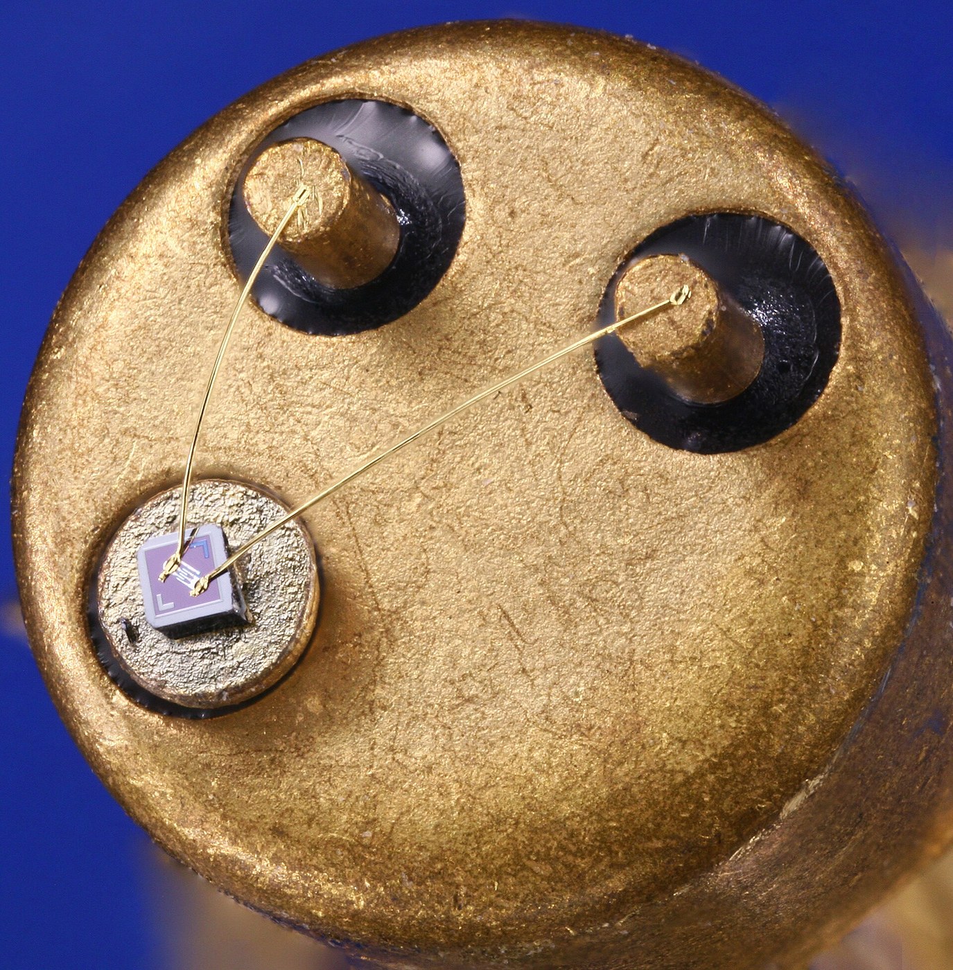


The Planar Process
By 1958 the industry could purify silicon, grow it as a single crystal, mask it with oxide, dope it through windows and pattern those windows with light. It could make a transistor. It could not make a transistor that reliably still worked six months later.
The problem was the edge. Transistors were built as mesas: diffuse the layers across the wafer, then etch away everything around each device so it stood on a plateau, which cut the junctions loose from their neighbours. That etch exposed the junction at the mesa sidewall, and a junction exposed to the air is a disaster. Surface states trap charge, moisture and sodium ions drift across it, leakage current wanders with humidity and temperature, and devices degrade unpredictably. Manufacturers hermetically sealed each transistor in a metal can with a nitrogen atmosphere and still lost yield to it.
Jean Hoerni at Fairchild wrote the answer in his notebook in December 1957 and filed it in May 1959, and it is one of those ideas that sounds like nothing until you see what it removes.
Do not etch the oxide off.
That is it. The oxide is already there, because you grew it to mask the diffusion. Every previous process treated it as scaffolding and stripped it once it had done its job. Hoerni left it in place. The junction now terminates not at a raw etched sidewall but underneath a continuous layer of thermally grown glass, which is chemically inert, mechanically hard, and bonded to the silicon with remarkably few electrically active states. The junction is sealed at the moment it is created and never sees the air at all.
The consequences went far beyond reliability, and this is why the process rather than the device is the historic object. The wafer surface is now FLAT — planar — so you can evaporate a metal film over the whole thing and photolithographically pattern it into wires that run across the oxide from one device to another without shorting to the silicon beneath. Hoerni solved a leakage problem and handed Robert Noyce the integrated circuit.
고급
5 hours
안내
1
1
Why an exposed junction fails, and how to see it happen
Why an exposed junction fails, and how to see it happen
Hoerni's fix only makes sense if you understand what it was fixing, and surface leakage is invisible until you measure it.
WHAT GOES WRONG AT A BARE SURFACE. Inside the crystal every silicon atom has four neighbours and four satisfied bonds. At a surface the lattice simply stops, leaving unsatisfied bonds — dangling bonds — that sit at energies inside the forbidden gap and can trap or release charge. A trapped charge is an electric field, and an electric field at the surface of a junction bends the bands and creates a conducting channel along the surface where none was designed. Current leaks around the junction rather than through it.
Worse, the surface charge is not fixed. Water vapour adsorbs and desorbs. Sodium ions — from fingerprints, from glassware, from the air — are small and mobile and drift under any applied field, so the leakage changes as the device is used and changes again when it is switched off. This is why early transistors had reputations rather than specifications.
WHAT THE OXIDE DOES. A thermally grown oxide satisfies most of those dangling bonds by bonding to them. The residual interface state density on a well-grown, hydrogen-annealed silicon-silicon dioxide interface is around 10^10 per square centimetre, against roughly 10^15 atoms per square centimetre at the surface — so fewer than one site in a hundred thousand remains electrically troublesome. Nothing else in materials science comes close, and it is specific to this one pairing.
SEE IT FOR YOURSELF, WITH A DIODE. You cannot fabricate a junction, but you can demonstrate that surface condition changes leakage, on any ordinary silicon diode with a glass body.
Set up a reverse-bias leakage measurement: diode reverse-biased through a large resistor, say 10 megohms, from a 9 V supply, with your multimeter measuring the voltage across the resistor. Reverse leakage in a small signal diode is nanoamps, so across 10 megohms that is tens of millivolts — measurable.
Now change the surface and watch the reading. Breathe on the glass body: the reading moves as moisture condenses, then drifts back as it evaporates. Handle the body with bare fingers and measure again; the salt and oil from a fingerprint is a conductive film and an ion source. Warm it gently with a hairdryer and watch leakage climb — some of that is genuine thermal generation, which doubles roughly every 8 to 10 degrees, but the surface contribution is what recovers slowly rather than instantly when you stop heating.
What you are watching is a device whose junction is sealed inside glass, and it STILL responds to what happens on its outside surface. Now imagine the junction itself exposed. That is the mesa transistor, and that is what Hoerni buried.
이 단계의 재료:
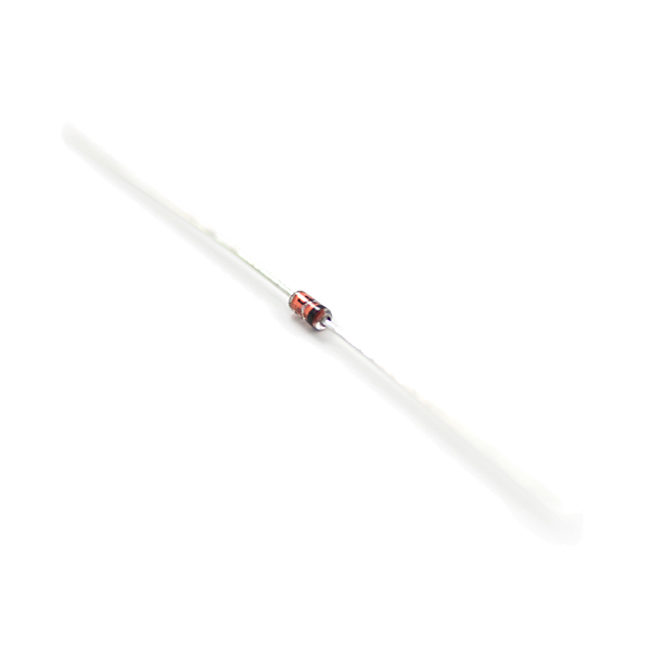 Diode Small Signal - 1N414810 개
 저항 키트1 세트
 배럴잭 리드가 달린 9 V 건전지1 개
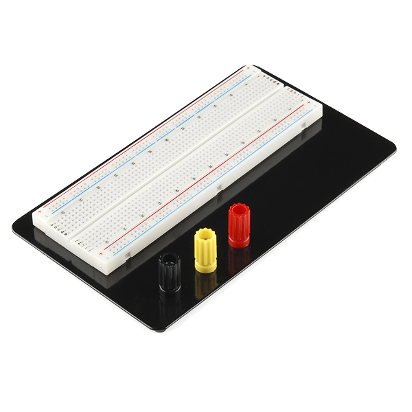 Breadboard1 개
필요한 도구:
 실험실급 디지털 멀티미터
 실험용 온도계
 스톱워치
스톱워치2
2
The full planar sequence, and what each mask costs
The full planar sequence, and what each mask costs
A planar bipolar transistor takes five masks. Every one is a full photolithography cycle — coat, expose, develop, etch, strip — and every one must register to the ones before it.
The diagram lays out the sequence. Read it as an accounting exercise as much as a process: each mask is a cost, a yield risk and an alignment tolerance, and the entire subsequent history of the industry is about getting more function out of each one.
Two features of the sequence deserve attention because they are not obvious.
ISOLATION WITHOUT ETCHING. The mesa process separated devices physically. Planar does not separate them at all — every device sits in the same continuous piece of silicon. What keeps them from shorting is that each device sits in its own island of one doping type surrounded by the opposite type, and the junction between them is reverse-biased in operation. A reverse-biased junction passes almost no current, so it acts as an insulator. This is junction isolation, it costs one extra diffusion and a lot of area, and it is why the first integrated circuits had so few components on so much silicon.
THE OXIDE REGROWS ITSELF. You never explicitly grow oxide after the first time. Each diffusion happens in an oxidising ambient, so the window you opened has sealed over by the time the diffusion finishes. The process is self-sealing, which is exactly the property that makes it reliable, and it falls out of the physics rather than being engineered in.
Flow
Loading...
3
3
Yield — the arithmetic that decides whether any of this is a business
Yield — the arithmetic that decides whether any of this is a business
Jupyter 노트북 불러오는 중…
필요한 도구:
 데스크톱 컴퓨터
4
4
Compendium — what Hoerni actually handed over
Compendium — what Hoerni actually handed over
WAS THE PLANAR PROCESS OBVIOUS? It looks obvious now, which is the usual fate of a good idea. At the time the oxide was universally regarded as a nuisance to be removed once it had served as a diffusion mask, partly because nobody was certain it was not itself a source of contamination. Hoerni's contribution was to recognise that the layer everyone was throwing away was the solution to the problem everyone was fighting. His notebook entry is dated 1 December 1957; he did not build one until 1958 because Fairchild was busy shipping mesa devices.
WHY DID EPITAXY BECOME PART OF IT? A transistor wants a lightly doped collector for high breakdown voltage but a heavily doped path to the contact for low resistance, and one uniformly doped wafer cannot be both. Epitaxy — growing a fresh, lightly doped single-crystal layer on top of a heavily doped substrate — gives you both in one wafer, with the layer taking its crystal orientation from the substrate beneath. It arrived in 1960, a year after planar, and the two together are what people usually mean by the planar process today.
WHAT IS THE REAL COST OF JUNCTION ISOLATION? Area, capacitance and leakage. Every isolated island needs a diffused wall around it, and that wall must be wide enough to allow for lateral diffusion, so a large fraction of early IC area was isolation rather than device. The isolation junction also has capacitance to the substrate, which slows the circuit, and it leaks a little, which matters in low-power designs. It was eventually replaced by dielectric isolation — oxide-filled trenches — which costs process steps instead of area.
WHY ALUMINIUM FOR THE METAL? It adheres well to silicon dioxide, it can be evaporated easily, it patterns cleanly with photolithography, and crucially it makes a good ohmic contact to silicon after a modest anneal. Its problems arrived later at scale: aluminium dissolves silicon at the contact, which can spike through a shallow junction, and at high current density the electron wind physically moves aluminium atoms along the wire until it thins and fails — electromigration. Both were managed with alloying and barrier layers before copper replaced aluminium in the late 1990s.
WHY IS THIS A PROCESS BLUEPRINT AND NOT A DEVICE ONE? Because the device is ordinary and the process is the invention. A planar transistor does exactly what a mesa transistor does, only reliably. What Hoerni actually created was a manufacturing method with three properties nobody had had together: junctions sealed at birth, a flat surface, and complete compatibility with photolithographic patterning. The next two blueprints are what other people did with those three properties within eighteen months.
재료
4- Diode Small Signal - 1N414810% 수수료10 개₩3
- 플레이스홀더
- 플레이스홀더
- Breadboard - Classic10% 수수료1 개₩127
예상 총액
만든 사람이 산 것. 가격이 없는 재료는 구매하는 곳에서 구하면 됩니다.
관련 블루프린트
이 블루프린트들은 지식을 공유합니다 — 기술, 재료 또는 원리


CC0 퍼블릭 도메인
이 블루프린트는 CC0로 공개되었습니다. 어떤 목적으로든 자유롭게 복사, 수정, 배포 및 사용할 수 있습니다.
제품 구매를 통해 메이커를 지원하세요. 판매자가 설정한 메이커 커미션 을 받거나, 이 블루프린트의 새로운 반복을 만들어 연결로 포함시킬 수 있습니다.