အနုပညာ
အလှအပနှင့် ကျန်းမာရေး
လက်မှုအနုပညာ
ယဉ်ကျေးမှုနှင့် သမိုင်း
ဖျော်ဖြေရေး
ပတ်ဝန်းကျင်
အစားအစာနှင့် အချိုရည်
ပြောင်းပြန်အင်ဂျင်နီယာပညာ
သိပ္ပံပညာများ
အားကစား
နည်းပညာ
ဝတ်ဆင်နိုင်သောပစ္စည်းများ

Photolithography
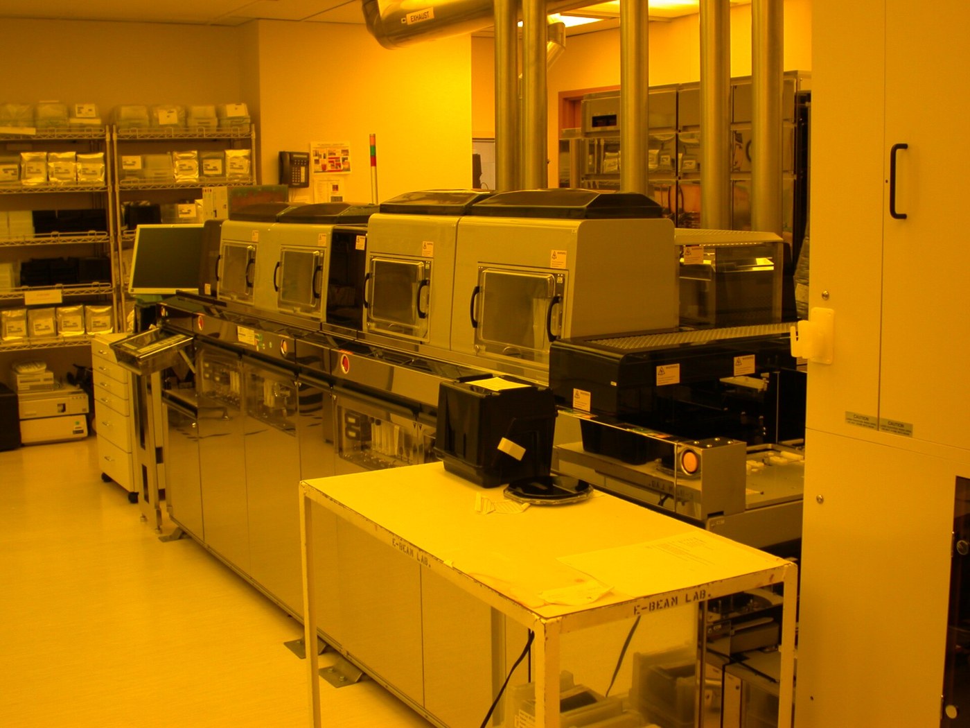
The oxide mask told you WHERE the dopant may enter. This blueprint is about how the window gets cut, and it is the step that turned a laboratory process into an industry — because it is the only one that scales.
Everything else in semiconductor manufacture treats the whole wafer at once. The furnace heats every device equally; the diffusion doses them all together. Only patterning has to distinguish one square micrometre from its neighbour, millions of times over, and do it in the same time whether there are ten features or ten billion.
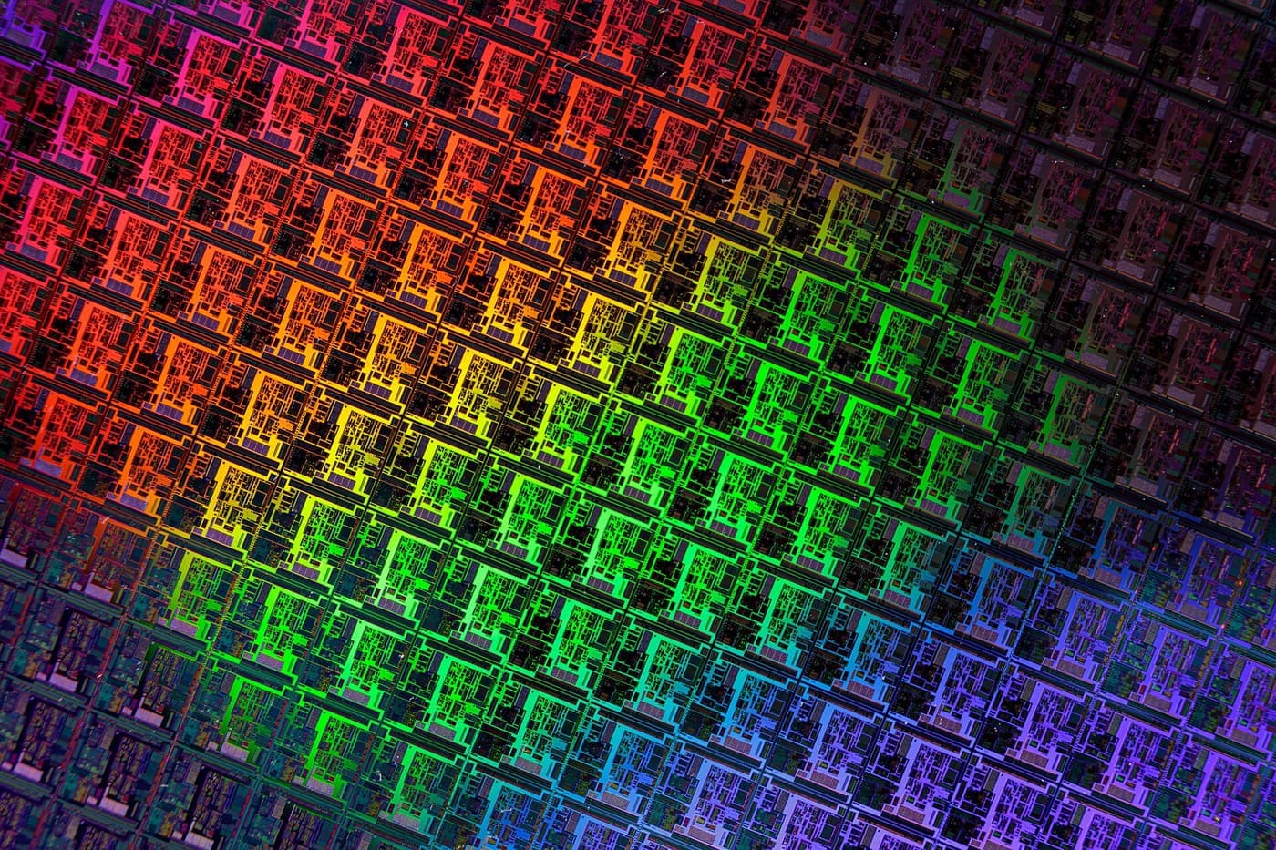
Jules Andrus at Bell Labs filed the answer in 1957. Coat the oxidised wafer with a light-sensitive polymer. Shine light through a mask carrying the pattern. Where light lands, the polymer changes its solubility. Develop away the parts you no longer want, etch the oxide through the openings, strip what remains, and you have transferred a drawing into a material — in one exposure, for every feature at once.
That last clause is the whole economic argument for the integrated circuit. A million transistors cost no more to pattern than one, because the light does not care. Everything about the industry's cost curve descends from it.
The first resists were cyclised rubber, sensitised by dichromate — Kodak's KTFR, a direct descendant of nineteenth-century photoengraving chemistry, which is where Andrus took it from. Resolution was tens of micrometres. Sixty years later the same five operations run at a few nanometres.
And this is the one step in this batch you can do for real. Dry-film photoresist on copper-clad board is the same chemistry, the same five operations and the same failure modes as the industrial process, at a resolution of about 100 micrometres instead of 5 nanometres. You will pattern something, measure your own minimum resolvable line, and then work out from the physics exactly what separates your result from a modern fab.
အလယ်အလတ်
6 hours
ညွှန်ကြားချက်များ
1
1
The five operations, and the fact that they never change
The five operations, and the fact that they never change
Photolithography is five operations in a fixed order, repeated once per layer. A modern chip runs this cycle 60 to 100 times, and the sequence has not changed since 1957 — only the wavelength, the resist chemistry and the machinery.
COAT. Put a uniform film of photoresist on the wafer. Industrially this is a spin coater: a few millilitres dropped on the centre while the wafer spins at 3000 rpm, throwing off the excess and leaving a film whose thickness depends on spin speed and viscosity. Uniformity matters because exposure dose and development time are set for one thickness.
EXPOSE. Project or contact-print the mask pattern onto the resist. Positive resist becomes MORE soluble where light strikes; negative resist becomes LESS soluble, by cross-linking. Both are used, for different reasons.
DEVELOP. Wash away the soluble regions in a developer — a mild alkali for most resists. What remains is a resist stencil sitting on the oxide.
ETCH. Remove the oxide where the resist is absent. Wet etching uses buffered hydrofluoric acid and attacks in all directions equally, so it undercuts the resist. Dry etching uses a plasma and can be made directional, which is what allows small features.
STRIP. Remove the remaining resist, leaving patterned oxide. Then the next layer begins.
The diagram shows the cycle, the two resist polarities, and the four things that limit how small a feature can be — because those four are the entire story of the industry's roadmap.
Flow
Loading...
2
2
Run all five for real, on copper
Run all five for real, on copper
Dry-film photoresist on copper-clad board runs the identical five operations with equipment you can buy for the price of a meal. Do it properly and measure the result rather than admiring it.
MAKE THE MASK. Print your pattern on inkjet transparency film at the highest density your printer manages, or better, print two identical copies and stack them in register to double the optical density — thin ink is the commonest cause of a washed-out image, because resist responds to total dose and grey is not black. Design the pattern as a resolution test: a series of line-and-space pairs at 500, 400, 300, 250, 200, 150, 100, 80 and 50 micrometres, plus some large areas and some isolated dots. You are not making a circuit, you are measuring your process.
PREPARE THE SUBSTRATE. Scrub the copper with a fine abrasive block, rinse, degrease with isopropanol, and dry. From here handle by the edges only. Fingerprints are grease, grease stops resist adhering, and every void in your pattern will sit exactly where a finger was.
COAT. Peel the matte protective layer from the dry film and laminate it onto the warm copper — a domestic laminator at about 100 degrees, two passes. You are aiming for no trapped air. Bubbles become holes.
EXPOSE. Sandwich mask against resist under a sheet of clean glass, emulsion side down and in firm contact, and expose to UV. A 365 nm LED array or an unfiltered fluorescent UV tube works. Contact is critical and it is worth pressing hard: any air gap lets light diffract around the mask edge, and the penumbra that results is the difference between a 100 micrometre line and a smear.
Bracket the dose. This is the single most useful thing you will do. Expose a strip of identical test patterns for 30, 60, 90, 120, 180 and 240 seconds by sliding an opaque card along in steps. Underexposed negative resist washes away entirely; overexposed resist spreads, because scattered light reaches beyond the mask edge and lines close up. There is a window, it is narrower than people expect, and you cannot find it by reasoning.
DEVELOP. Sodium carbonate solution, about 1 percent, at 30 degrees, with gentle agitation. Watch it: unexposed film lifts and clears in 30 to 90 seconds. Stop as soon as the copper is clean, because the developer slowly attacks the exposed resist too and over-development thins your lines.
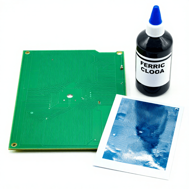
ETCH. Ferric chloride, or the hydrogen-peroxide-and-hydrochloric-acid mixture. Warm and agitated etches faster and, importantly, more evenly. Wear goggles and gloves and work over a sink; ferric chloride stains everything it touches permanently.
STRIP. Stronger sodium hydroxide, 3 to 5 percent, lifts the cured resist in a minute or two.
MEASURE. Under the microscope with a calibrated scale, find the finest line and space pair that came out cleanly separated and correctly sized. That number is your critical dimension, and it is the honest output of this step. 100 to 150 micrometres is a good result on a first attempt with a domestic laminator and an inkjet mask.
Then measure the ERROR as well as the size. Compare the width of your developed 500 micrometre line against the mask. It will not be 500. Wet etching removes copper sideways as fast as downwards, so a line etched through 35 micrometres of copper loses about 35 micrometres from each side. That is undercut, it is limit 4 from the previous step, and you have just measured it.
ဤအဆင့်အတွက် ကုန်ကြမ်းများ:
 ခြောက်သွေ့ဖလင် ဖိုတိုရေစစ်1 ခု
 လျှပ်စီးကြောင်းပြားအလွတ် (ကြေးနီဖုံး)4 ခု
 ဆိုဒီယမ်ကာဗွန်နိတ် (ဆိုဒါပြာ)250 gram
 အက်ဆစ်ထွင်းဆေးရည် (ဖယ်ရစ်ကလိုရိုက်)1 လီတာ
 ခရမ်းလွန်ရောင်ခြည် LED အစုံ1 ခု
လိုအပ်သော ကိရိယာများ:
 အပူသုံး ပလပ်စတစ်ဖုံးစက်
 ဒစ်ဂျစ်တယ် အဏုကြည့်မှန်ပြောင်း
 ဓာတ်ခွဲခန်း ဘေးကင်းရေးမျက်မှန်
 ဓာတုခံနိုင်သောလက်အိတ်
 အချိန်တိုင်းနာရီ
 ဒစ်ဂျစ်တယ် ကာလီပါ ၆ လက်မ
 အိုင်ဆိုပရိုပိုင် အရက်ပြန် ၉၉ %
 ဆိုဒီယမ်ဟိုက်ဒရောက်ဆိုဒ် — ဓာတ်ခွဲခန်းအဆင့်
 မင်ပက်ဖြန်းပုံနှိပ်စက်သုံး ကြည်လင်ဖလင်
3
3
Rayleigh, and the road from your 100 micrometres to their 5 nanometres
Rayleigh, and the road from your 100 micrometres to their 5 nanometres
Jupyter မှတ်စုစာအုပ် ဖွင့်နေသည်…
လိုအပ်သော ကိရိယာများ:
 စားပွဲတင်ကွန်ပျူတာဒစ်ဂျစ်တယ် အဏုကြည့်မှန်ပြောင်း
4
4
Alignment — the problem that only appears on the second layer
Alignment — the problem that only appears on the second layer
One patterned layer is a printing exercise. Two is semiconductor manufacturing, and the difference is registration.
Every layer after the first must land in a defined position relative to the ones already there. A transistor gate that sits 200 nanometres off its channel is not a slightly worse transistor, it is a short circuit. The tolerance on this — overlay — is typically a fifth to a third of the critical dimension, so a 5 nanometre process needs layer-to-layer alignment to about 1 nanometre, across a 300 millimetre wafer, at temperature.
DEMONSTRATE IT YOURSELF, because it is far harder than it sounds. Take a fresh board and run the process twice. First layer: a pattern of large crosses and a grid of 200 micrometre squares. Strip, re-laminate fresh resist, and expose a second mask carrying complementary crosses that should nest inside the first, and squares that should land exactly on the first set.
Then measure how far off you are. Under the microscope, measure the offset of the second-layer crosses from the first in x and y. You will not be at zero. A hand-aligned transparency on a domestic setup typically lands 100 to 500 micrometres out, and the sources are worth separating because each has an industrial counterpart:
TRANSLATION — the whole second layer is shifted. Simple positioning error. Industrially solved with an interferometric stage that knows its position to a fraction of a nanometre.
ROTATION — the offset grows along the board, in opposite directions at the two ends. You put the mask down at a slight angle. Industrially, the stage rotates to null it.
SCALE — the offset grows steadily from one edge to the other in the same direction. Your transparency has stretched, usually from the heat of the printer or the laminator, or the substrate itself has expanded. This is the interesting one: it is why fabs control temperature to a tenth of a degree, and why an inkjet transparency is fundamentally unsuitable for anything demanding. Measure the distance between your two outermost crosses on the mask and on the board and you can calculate the stretch directly, usually a few parts per thousand.
RUN-OUT AND DISTORTION — the offsets vary in a way that is neither uniform, rotational nor linear. Non-flat substrate, non-flat mask, or local stretch. Industrially this is corrected with high-order distortion terms, and residual distortion is one of the practical limits on overlay today.
What you should take away is that the alignment error is not one number, it is a FIELD, and separating it into these components is how you fix it rather than merely notice it. That analysis is identical in kind to what a modern lithography tool does between every wafer, from measurements on dedicated alignment marks placed around the die for exactly this purpose.
And the count matters. A modern chip needs 60 to 100 patterned layers, every one registered to those before it. If each layer yields 99.9 percent, a hundred layers yield 90 percent. That arithmetic — small errors compounding over many steps — is the real reason semiconductor fabrication is difficult, and it is a far better explanation of the industry's structure than the size of the features.
ဤအဆင့်အတွက် ကုန်ကြမ်းများ:
ခြောက်သွေ့ဖလင် ဖိုတိုရေစစ်1 ခုလျှပ်စီးကြောင်းပြားအလွတ် (ကြေးနီဖုံး)4 ခုအက်ဆစ်ထွင်းဆေးရည် (ဖယ်ရစ်ကလိုရိုက်)1 လီတာလိုအပ်သော ကိရိယာများ:
ဒစ်ဂျစ်တယ် အဏုကြည့်မှန်ပြောင်းဒစ်ဂျစ်တယ် ကာလီပါ ၆ လက်မအပူသုံး ပလပ်စတစ်ဖုံးစက်ဓာတုခံနိုင်သောလက်အိတ်မင်ပက်ဖြန်းပုံနှိပ်စက်သုံး ကြည်လင်ဖလင်5
5
Compendium — and how this differs from PCB etching
Compendium — and how this differs from PCB etching
HOW IS THIS DIFFERENT FROM THE PCB ETCHING BLUEPRINT? Honestly: the bench procedure in step 2 IS PCB etching, and that blueprint is linked from this one deliberately. The difference is what the procedure is being used to teach and where it is pointed. There, the aim is a working circuit board and the process is the means. Here, the aim is the process itself — you build a resolution test rather than a circuit, you bracket the exposure to find the window, you measure undercut and overlay as numbers, and every one of those numbers is then placed against the industrial equivalent. If you want a board, follow that blueprint. If you want to understand why a lithography tool costs as much as an aircraft, follow this one. Both use the same chemicals, and that is the point of having both.
WHY POSITIVE RESIST WON. Negative resists cross-link, and cross-linked polymer SWELLS when the developer soaks it, which distorts small features and limits resolution. Positive resists dissolve rather than swell. Negative resist was standard through the 1960s because it was more sensitive and more durable; positive took over as features shrank below a few micrometres and swelling became the binding limit. Modern chemically-amplified resists are a further generation again, where one photon triggers an acid that catalyses many reactions, buying the sensitivity back.
WHY IS 193 NANOMETRES STILL EVERYWHERE? Because the step past it was a cliff. At 157 nanometres, fused silica stops transmitting usefully and the programme was abandoned. The next viable wavelength is 13.5 nanometres, where nothing transmits at all — so EUV uses reflective optics of forty-plus alternating layers, in vacuum, with light made by hitting tin droplets with a CO2 laser fifty thousand times a second. Everything not requiring the finest features is still done at 193 nanometres because it works and it is paid for.
WHAT IS MULTIPLE PATTERNING? A way of beating the Rayleigh limit with two exposures instead of one. Print alternate lines in two separate passes, each individually within the resolution limit, interleaved to give a pitch neither could reach alone. It works, it doubles or quadruples the cost and time of that layer, and it makes overlay error a direct contributor to line placement. It is why EUV was worth its price.
WHY ARE MASKS 4x LARGER THAN THE PRINT? Projection tools demagnify, typically by four. Making the mask four times oversize eases the mask-making tolerance by the same factor, and shrinks the apparent size of any defect on it. The cost is field size: the exposed area is a fraction of the wafer, so the tool steps across the wafer exposing one field at a time. That is what a stepper steps.
WHAT IS THE PELLICLE? A thin transparent membrane held a few millimetres off the mask surface. Dust that lands on it is far outside the focal plane and images as a harmless blur rather than a printed defect. A simple, cheap idea that saved the industry an enormous amount of scrap, and a good example of solving a defect problem with geometry instead of cleanliness.
WHAT DID ANDRUS ACTUALLY CHANGE? He made patterning parallel. Before photolithography, features were placed one at a time, by hand or by mechanical mask. After it, every feature on the wafer is defined in a single exposure and the cost per feature falls as features multiply. Every subsequent economic fact about semiconductors — that transistors became effectively free, that complexity got cheaper rather than more expensive — descends from that one property.
ပစ္စည်းများ
5- နေရာယူပစ္စည်း
- နေရာယူပစ္စည်း
- 250 gramနေရာယူပစ္စည်း
- နေရာယူပစ္စည်း
- နေရာယူပစ္စည်း
လိုအပ်သော ကိရိယာများ
10- နေရာယူပစ္စည်း
- နေရာယူပစ္စည်း
- နေရာယူပစ္စည်း
- နေရာယူပစ္စည်း
- နေရာယူပစ္စည်း
- နေရာယူပစ္စည်း
- နေရာယူပစ္စည်း
- နေရာယူပစ္စည်း
- နေရာယူပစ္စည်း
- နေရာယူပစ္စည်း
ဆက်စပ် အစီအစဉ်များ
ဤအစီအစဉ်များသည် အသိပညာမျှဝေသည် — နည်းပညာ၊ ပစ္စည်း သို့မဟုတ် မူများ


CC0 အများပိုင်
ဤအစီအစဉ်ကို CC0 အောက်တွင် ထုတ်ဝေထားသည်။ ခွင့်ပြုချက်မလိုဘဲ ကူးယူ၊ ပြင်ဆင်၊ ဖြန့်ဝေ နှင့် အသုံးပြုနိုင်သည်။
အစီအစဉ်မှတစ်ဆင့် ကုန်ပစ္စည်းများဝယ်ယူ၍ လက်မှုပညာရှင်ကို ပံ့ပိုးပါ လက်မှုပညာရှင် ကော်မရှင် ရောင်းချသူက သတ်မှတ်သည်၊ သို့မဟုတ် ဤအစီအစဉ်၏ ဗားရှင်းအသစ်ဖန်တီး၍ ဝင်ငွေခွဲဝေရန် သင့်အစီအစဉ်တွင် ချိတ်ဆက်မှုအဖြစ် ထည့်သွင်းပါ။