IṢẸ́ ỌNÀ
ẸWÀ ÀTI ÌLERA
IṢẸ́ ỌWỌ́
ÀṢÀ ÀTI ÌTÀN
ÌṢERÉ
ÀYÍKÁ
OÚNJẸ ÀTI OHUN MÍMU
REVERSE ENGINEERING
SÁYẸ́ǸSÌ
ERÉ ÌDÁRAYÁ
ÌMỌ̀-Ẹ̀RỌ
ÀWỌN OHUN WÍWỌ̀
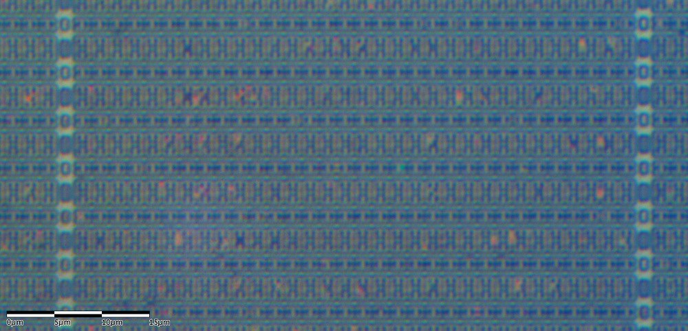

The SRAM Cell
This is the sibling of `dram-cell`. Same goal — hold one bit in silicon — and the opposite answer to every question.
DRAM stores charge on an isolated capacitor and accepts that the charge leaks, so it refreshes. SRAM stores the bit in a LOOP: two inverters wired output to input, each holding the other's input where it wants it. There is nothing to leak away, because nothing is isolated — the loop is connected to the supply and is actively driven. Cut the power and the bit is gone; leave the power on and it holds indefinitely with no maintenance at all.
That loop is not new. It is the Eccles-Jordan trigger of 1918, which this blueprint links back to, built from two valves. The same circuit, with MOSFETs, is a memory cell — and the fact that a 1918 valve circuit and a 2026 cache cell are the same topology is worth sitting with.
What it costs is transistors. Four for the loop and two more to connect it to the bit lines, against DRAM's one transistor and one capacitor. In area terms that is roughly six to one, and area is cost, which is why your computer has gigabytes of DRAM and megabytes of SRAM rather than the other way round.
What it buys is speed and simplicity. There is no refresh to schedule, no charge to share, no sense amplifier straining to read forty millivolts. The cell drives the bit line actively, so access is several times faster, and the cell is compatible with an ordinary logic process — which is why SRAM lives ON the processor die and DRAM lives on separate chips made in a different kind of factory.
You will build a cell from ordinary logic, prove that it holds without refresh, and then find its stability limit — the point at which a disturbance flips the bit — which is the number that actually constrains how small an SRAM cell can be made.
Ilọsíwájú
5 hours
Ìlànà
1
1
The six transistors, and the fight between them
The six transistors, and the fight between them
Look at the schematic and identify the three jobs.
M1 and M2 are one inverter: a p-channel pull-up and an n-channel pull-down with their gates tied. M3 and M4 are the other. The output of each feeds the input of the other, so if Q is high then QBAR is driven low, which drives Q high. The loop reinforces itself and that is the stored bit.
M5 and M6 are access transistors, gated by the wordline. They do nothing except connect the two internal nodes to the bit lines when the row is selected. They store nothing.
NOW THE PART THAT MAKES SRAM DESIGN HARD, and it is visible in the schematic as a conflict between two requirements on the same devices.
To READ, you raise the wordline and let the cell drive the bit lines. But raising the wordline also connects the bit lines — which are pre-charged high — to the internal node holding a 0. Charge flows in and lifts that node. If it lifts far enough to pass the other inverter's switching threshold, the loop flips and you have destroyed the bit by reading it. To prevent that, the pull-down transistor must be STRONGER than the access transistor, so it can hold the node down against the incoming charge. That ratio, M2 over M5, is the cell ratio, and it needs to be above roughly 1.5.
To WRITE, you drive the bit lines to the value you want and raise the wordline, and now you NEED the cell to flip. The access transistor has to overpower the pull-up holding the node high. So the access transistor must be STRONGER than the pull-up: the pull-up ratio, M1 over M5, needs to be below roughly 1.8.
Read stability wants the access transistor weak. Write ability wants it strong. Those are the same transistor. Every SRAM cell ever designed is a point chosen inside that conflict, and it gets harder as devices shrink because random variation in threshold voltage — which grows as the channel gets smaller — eats the margin from both sides at once. That is the real reason SRAM has struggled to scale, and why some designs use eight transistors to separate the read path from the write path and buy the conflict away with more area.
Ń gbé olùwò KiCanvas wọlé...
Olùwò Àpẹrẹ PCB Akọ́ṣẹ́mọṣẹ́
Àwọn irinṣẹ́ tí a nílò:
 Kọ̀ǹpútà Tábìlì
2
2
Build the loop and prove it needs no refresh
Build the loop and prove it needs no refresh
You cannot build six matched MOSFETs on a breadboard with useful ratios. You can build the loop, which is the part that matters, and the comparison against the DRAM cell is direct and stark.
THE BUILD. Two inverters from a 74HC04, output of the first to input of the second and back again. That is the storage loop. Two more pins for the access path: a 74HC4066 analogue switch on each node, both controlled by one line, which is your wordline. LEDs with 1 kilohm resistors on each node so you can see the state.
WRITE A BIT. Close the switches with the bit lines driven — one high, one low — and the loop takes that state. Open the switches. The LEDs stay as they are.
NOW THE COMPARISON, and it is the whole point of building this alongside the DRAM cell. Leave both circuits powered and untouched.
The DRAM cell loses its bit in seconds. You measured its half-life and watched it die on the scope.
The SRAM cell does not change. Come back in an hour, a day, a week. As long as the supply is present the LEDs are exactly as you left them, because the loop is actively driving itself and there is no isolated node for charge to leak off.
That is the entire difference between static and dynamic, demonstrated on two breadboards side by side.
NOW PULL THE POWER, briefly. Both lose everything. Both are volatile — that is what SRAM does NOT buy you, and it is worth being explicit because people conflate static with non-volatile. Core memory in the previous blueprint keeps its bits with the power off. Neither of these does. The floating gate two blueprints from here is the one that solves that, and it took until 1971.
FIND THE STABILITY LIMIT. Take a 10 kilohm potentiometer between one node and the opposite rail and wind it down slowly, injecting a disturbance into a node the loop is trying to hold. At some resistance the loop gives up and flips. Record it, and repeat several times — it should be repeatable to within a few percent.
That resistance is a crude measure of static noise margin: how big a disturbance the cell tolerates before losing the bit. Convert it to a voltage by measuring the node voltage just before it flips. In a real cell that margin is a few hundred millivolts at best, and it shrinks with supply voltage and with device variation, which is why SRAM stops working at low voltage before logic does.
Àwọn ohun èlò fún ìgbésẹ̀ yìí:
 Onírúurú IC lóògíìkì1 ìtò
 Onírúurú LED1 ìtò
 Àkójọ Rẹsístà1 ìtò
 Oríṣiríṣi potentiometer1 ìtò
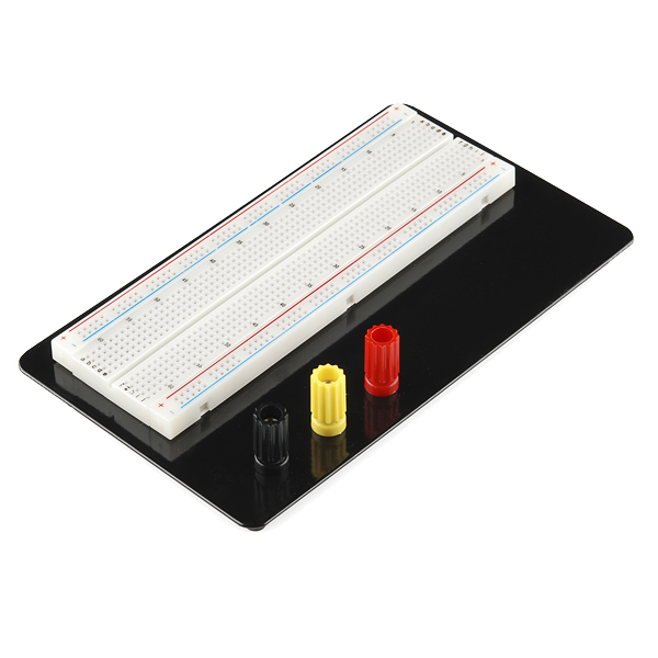 Breadboard2 ẹyọ
 Àkójọ Okùn Ìsopọ̀1 ìtò
Àwọn irinṣẹ́ tí a nílò:
 Òsílóskóòpù
 Òṣùwọ̀n Oníṣirò Díjítà Ìpele Yàrá Ìwádìí
 Ìpèsè Agbára Tábìlì
 Aago Ìdúró
3
3
The butterfly curve, and why the cell has a stability limit at all
The butterfly curve, and why the cell has a stability limit at all
Ń ṣí ìwé Jupyter…
Àwọn irinṣẹ́ tí a nílò:
Kọ̀ǹpútà TábìlìÀwọn ohun-èlò
6- 1 ìtòÀyè
- 1 ìtòÀyè
- Àyè
- Àyè
- Breadboard - Classicìdá 10%2 ẹyọ$9.38
- 1 ìtòÀyè
Àwọn irinṣẹ́ tó nílò
5- Àyè
- Àyè
Àpapọ̀ Ìfojúsùn
Ohun tí ẹni tó ṣe é rà. Àwọn ohun èlò tí kò ní iye owó ni o máa rà níbi tí o bá ti rà á.
Blueprint tó jọra
Àwọn blueprint wọ̀nyí pín ìmọ̀ — ọ̀nà, ohun-èlò tàbí ìlànà

CC0 Àgbègbè Gbogbogbò
Blueprint yìí ti jáde lábẹ́ CC0. O lè ṣe àdàkọ, yí padà, pín, àti lò láìsí ìyọ̀ǹda.
Ṣàtìlẹ́yìn Olùṣẹ́dá nípa rírà àwọn ọjà nipasẹ̀ Blueprint wọn Ẹ̀san Olùṣẹ́dá tí àwọn Olùtajà gbé kalẹ̀, tàbí ṣẹ̀dá àtúnṣe tuntun ti Blueprint yìí kí o sì fi sínú Blueprint rẹ gẹ́gẹ́ bí ìsopọ̀ láti pín owó-wíwọlé.