Pakikipagtulungan
SINING
BEAUTY AT WELLNESS
CRAFTS
KULTURA AT KASAYSAYAN
LIBANGAN
KAPALIGIRAN
PAGKAIN AT INUMIN
REVERSE ENGINEERING
AGHAM
ISPORTS
TEKNOLOHIYA
MGA WEARABLE
Ang On-Chip SRAM: Isang Humihingang Ilaw na Nakaimbak sa Sariling Memorya ng Iyong Chip
English
Youblob (simulation output) · CC0
Ed

Nilikha ni

Ed

29. Setyembre 2026FI
49
0
0
0
0

Ang On-Chip SRAM: Isang Humihingang Ilaw na Nakaimbak sa Sariling Memorya ng Iyong Chip

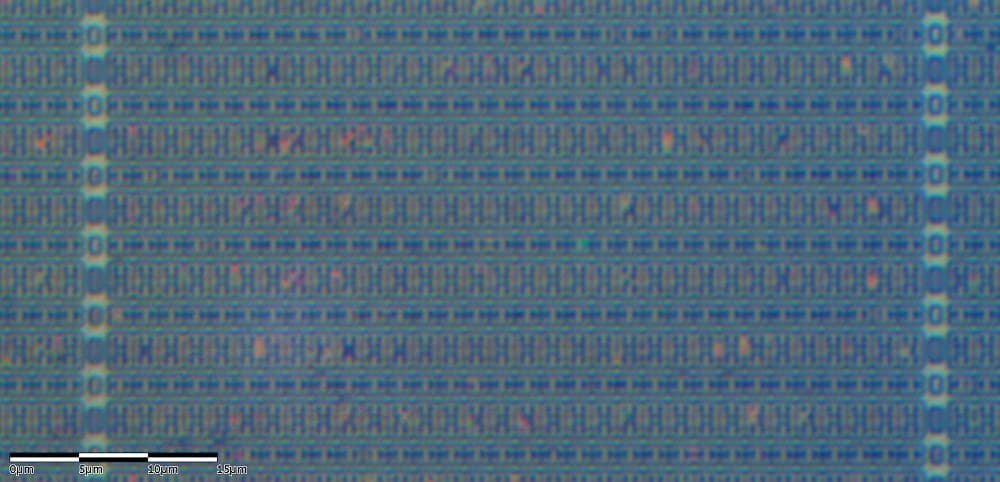
Ang template ng wafer.space ay may kasamang dalawang SRAM macro sa kanilang halimbawang disenyo, tig-512 bytes bawat isa, at iniwan itong naka-patay. Ang macro ay isang tapos nang bloke ng memorya mula sa PDK: 4,096 na static memory cell, na iginuhit nang isang beses kasama ang kanilang address decoder at read circuit, at inilalagay mo nang buo sa halip na buuin mula sa mga gate. Binubuksan ng rung na ito ang isa sa mga ito. Ang PWM dimmer mula sa naunang rung ay nagpapatugtog na ngayon ng isang pattern: isinusulat ng microcontroller ang 256 bytes sa chip sa pamamagitan ng mga pad nito, minsan lang, at mula noon ay binabasa ng chip ang mga ito nang mag-isa, isang byte bawat hakbang, bilang liwanag ng isang dahan-dahang humihingang ilaw. Ang core at ang testbench nito ay pinatakbo para sa blueprint na ito gamit ang Icarus Verilog 12.0, cocotb 2.1.0 at ang sariling simulation model ng PDK para sa SRAM macro: sinundan ng output ang nakaimbak na talahanayan sa loob ng 600 PWM period. Ang larawan ay sariling output ng simulation na iyon, isang bar bawat period. Ang ESP32 sketch na naglo-load ng talahanayan ay na-compile para sa blueprint na ito; wala pang chip na mapapatakbuhan nito.
Abantado
Isang gabi, kasama ang chip

Mga Tagubilin

1

Ang pattern, ang timing at ang laki

Naglo-load ng Jupyter notebook…
2

Ano ang bawat isa sa 4,096 bits

Ipinapakita ng naka-embed na blueprint kung paano hinahawakan ng isang bit ng static memory ang sarili nito: isang loop ng dalawang inverter. Ang macro sa rung na ito ay 4,096 bits ng static memory sa iisang array.
3

Ang mga pin ng macro, at tatlong bagay na sinasabi ng model nito

gf180mcu_fd_ip_sram__sram512x8m8wm1 ay may hawak na 512 bytes. Ang mga pin nito: CLK; A, isang 9-bit na address; D, ang byte na isusulat; Q, ang byte na binasa. Ang tatlong control ay pawang active LOW. Ang CEN na 0 ay nagbubukas ng memory. Ang GWEN na 0 ay ginagawang write ang clock edge, at read naman kapag 1. Ang WEN ay may isang bit bawat data bit, at ang 0 ay nagpapahintulot na maisulat ang bit na iyon, kaya maaaring baguhin ng write ang ilang bit ng isang byte at iwanang hindi nagalaw ang iba. Sa pagbasa ng simulation model ng PDK, may tatlong bagay na dapat malaman. Una, gumagana lamang ang memory pagkatapos mapunta ang CEN mula 1 patungong 0; kung hindi, ipiprint ng model ang "CEN is not reset, memory is not operational", kaya pinananatili ng core ang CEN sa 1 habang nagre-reset at ibinababa ito pagkatapos. Ikalawa, ang read ay nagbibigay ng mem[A] sa Q pagkatapos ng clock edge na sumampol sa A, kaya handa na ang data makalipas ang isang clock. Ikatlo, nagsisimula ang model na may lahat ng byte na 0. Hindi ito ginagawa ng totoong chip: ang SRAM nito ay nagsisimulang may laman ang bawat cell na nahulugan nito, kaya dapat magsulat muna ang design bago magbasa. Ang sariling halimbawa ng template ay nagtatakda ng CEN sa 1, kaya nakapatay ang dalawang macro nito. Ayon sa timing files nito, ang pinakamababang clock period ng macro ay 6.6 ns sa typical na 5 V corner at 18.3 ns sa mabagal na 3.0 V, 125 °C corner, parehong nasa loob ng 40 ns ng template.
4

The core

src/chip_core.sv for the pattern player, with the template's port list unchanged plus one parameter, HOLD_LOG2. Input pad 0 enables, pad 1 selects LOAD mode, pad 2 is the write strobe; bidirectional pads 0 to 7 carry the byte, pad 8 the PWM. The LOAD and strobe pads are passed through two flip-flops before use, a synchroniser: they change whenever the outside world likes, not in step with the chip's clock, and a flip-flop caught mid-change can hover between 0 and 1 for a while. In play mode, each time HOLD_LOG2 periods have passed, the byte the SRAM has been reading becomes the new duty and the address moves on.
chip_core.svsystemverilog
// SPDX-License-Identifier: Apache-2.0
// Youblob silicon rung 5: the PWM dimmer plays a brightness pattern stored in the on-chip SRAM macro.
// Port list unchanged from wafer-space/gf180mcu-project-template src/chip_core.sv.

`default_nettype none

module chip_core #(
    parameter NUM_INPUT_PADS,
    parameter NUM_BIDIR_PADS,
    parameter NUM_ANALOG_PADS,
    parameter HOLD_LOG2 = 9        // each table entry lasts 2**HOLD_LOG2 PWM periods
    )(
    `ifdef USE_POWER_PINS
    inout  wire VDD,
    inout  wire VSS,
    `endif

    input  wire clk,       // clock
    input  wire rst_n,     // reset (active low)

    input  wire [NUM_INPUT_PADS-1:0] input_in,   // Input value
    output wire [NUM_INPUT_PADS-1:0] input_pu,   // Pull-up
    output wire [NUM_INPUT_PADS-1:0] input_pd,   // Pull-down

    input  wire [NUM_BIDIR_PADS-1:0] bidir_in,   // Input value
    output wire [NUM_BIDIR_PADS-1:0] bidir_out,  // Output value
    output wire [NUM_BIDIR_PADS-1:0] bidir_oe,   // Output enable
    output wire [NUM_BIDIR_PADS-1:0] bidir_cs,   // Input type (0=CMOS Buffer, 1=Schmitt Trigger)
    output wire [NUM_BIDIR_PADS-1:0] bidir_sl,   // Slew rate (0=fast, 1=slow)
    output wire [NUM_BIDIR_PADS-1:0] bidir_ie,   // Input enable
    output wire [NUM_BIDIR_PADS-1:0] bidir_pu,   // Pull-up
    output wire [NUM_BIDIR_PADS-1:0] bidir_pd,   // Pull-down

    inout  wire [NUM_ANALOG_PADS-1:0] analog  // Analog
);

    // Input pad 0: enable.  Input pad 1: LOAD mode.  Input pad 2: write strobe.
    // Bidir pads 0..7: the byte to store while loading.  Bidir pad 8: the PWM output.
    localparam DUTY_W = 8;
    localparam PWM_PAD = 8;

    assign input_pu = '0;
    assign input_pd = '0;
    assign bidir_oe = {{(NUM_BIDIR_PADS-DUTY_W){1'b1}}, {DUTY_W{1'b0}}};
    assign bidir_ie = ~bidir_oe;
    assign bidir_cs = {{(NUM_BIDIR_PADS-DUTY_W){1'b0}}, {DUTY_W{1'b1}}};
    assign bidir_sl = '0;
    assign bidir_pu = '0;
    assign bidir_pd = '0;

    wire enable = input_in[0];
    wire [DUTY_W-1:0] data_in = bidir_in[DUTY_W-1:0];

    // The mode and strobe pads change whenever the outside world likes, not in step with clk:
    // two flip-flops in a row (a synchroniser) before anything uses them.
    logic [1:0] load_s;
    logic [2:0] strobe_s;
    always_ff @(posedge clk) begin
        load_s   <= {load_s[0], input_in[1]};
        strobe_s <= {strobe_s[1:0], input_in[2]};
    end
    logic load_was;
    wire load        = load_s[1];
    wire load_start  = load & ~load_was;
    wire strobe_rise = strobe_s[1] & ~strobe_s[2];
    always_ff @(posedge clk) load_was <= load;

    // The SRAM wants its chip enable (CEN, active LOW) to go 1 -> 0 before it works:
    // hold it at 1 through reset, then 0.
    logic cen;
    always_ff @(posedge clk) cen <= !rst_n;

    // PWM counter and the "hold" counter that decides when to step to the next table entry.
    logic [DUTY_W-1:0] count;
    logic [HOLD_LOG2:0] hold;                   // one bit wider so HOLD_LOG2 = 0 still works
    wire period_end = (count == '1);
    localparam logic [HOLD_LOG2:0] HOLD_MASK = (1 << HOLD_LOG2) - 1;   // 0 when HOLD_LOG2 = 0
    wire step = period_end && ((hold & HOLD_MASK) == HOLD_MASK);

    logic [DUTY_W-1:0] addr;
    logic [DUTY_W-1:0] duty;
    wire  [DUTY_W-1:0] q;                       // SRAM read data: mem[addr], one clock after addr

    always_ff @(posedge clk) begin
        if (!rst_n) begin
            count <= '0;  hold <= '0;  addr <= '0;  duty <= '0;
        end else if (load) begin
            count <= '0;  hold <= '0;  duty <= '0;
            if (load_start)       addr <= '0;       // every load starts at entry 0
            else if (strobe_rise) addr <= addr + 1'b1;
        end else if (enable) begin
            count <= count + 1'b1;
            if (period_end) hold <= hold + 1'b1;
            if (step) begin
                duty <= q;                          // the entry that was being read
                addr <= addr + 1'b1;                // and move on to the next
            end
        end
    end

    `gf180mcu_xxx_ip_sram__sram512x8m8wm1 sram_0 (
        `ifdef USE_POWER_PINS
        .VDD  (VDD),
        .VSS  (VSS),
        `endif
        .CLK  (clk),
        .CEN  (cen),                                   // active low: 0 = on
        .GWEN (~(load && strobe_rise)),                // active low: 0 = write this clock
        .WEN  (8'b0),                                  // active low, per bit: write all eight
        .A    ({1'b0, addr}),                          // 256 of the 512 bytes
        .D    (data_in),
        .Q    (q)
    );

    logic pwm;
    always_ff @(posedge clk) begin
        if (!rst_n) pwm <= 1'b0;
        else        pwm <= enable && !load && (count < duty);
    end

    logic [NUM_BIDIR_PADS-1:0] out;
    always_comb begin
        out = '0;
        out[PWM_PAD] = pwm;
    end
    assign bidir_out = out;

    // Inputs this design does not read (keeps lint quiet, as the template does with _unused).
    logic _unused;
    assign _unused = &{1'b0, input_in[NUM_INPUT_PADS-1:3], bidir_in[NUM_BIDIR_PADS-1:DUTY_W], hold[HOLD_LOG2]};

endmodule

`default_nettype wire

Mga kailangang kasangkapan:

Desktop na KompyuterDesktop na Kompyuter
5

The test

test_pattern.py builds the core with the PDK's SRAM model, gf180mcu_fd_ip_sram__sram512x8m8wm1.v, at the template's 25 MHz and with HOLD_LOG2 = 0 so the whole table plays in 256 periods. It loads the table through the pads the way the ESP32 will, then counts the high clocks in each of 600 PWM periods and requires them to follow the table from exactly one starting point. A second test loads again and checks the new pattern replaced the old.
test_pattern.pypython
# SPDX-License-Identifier: Apache-2.0
# cocotb testbench for the SRAM pattern player, with the PDK's own SRAM simulation model
# (gf180mcu_fd_ip_sram__sram512x8m8wm1, gf180mcuD, the commit the template pins).
import math
import os
from pathlib import Path

import cocotb
from cocotb.clock import Clock
from cocotb.triggers import ClockCycles, FallingEdge, RisingEdge
from cocotb_tools.runner import get_runner

PWM_PAD = 8
EN, LOAD, STROBE = 1, 2, 4                      # input pad bits
SRAM = Path(os.getenv("PDK_ROOT", "pdk")) / "gf180mcuD" / "libs.ref" / "gf180mcu_fd_ip_sram" / "verilog"


def breathing_table(n=256, gamma=2.2):
    """One slow breath: a raised sine, gamma-corrected so equal steps LOOK equal to the eye."""
    return [round(255 * ((1 - math.cos(2 * math.pi * i / n)) / 2) ** gamma) for i in range(n)]


async def start(dut):
    cocotb.start_soon(Clock(dut.clk, 40, unit="ns").start())   # 25 MHz, the template's CLOCK_PERIOD
    dut.input_in.value = 0
    dut.bidir_in.value = 0
    dut.rst_n.value = 0
    await ClockCycles(dut.clk, 5)
    dut.rst_n.value = 1
    await ClockCycles(dut.clk, 2)


async def load(dut, table):
    """What a microcontroller on the breakout does: LOAD high, then per byte set the data pads,
    raise the strobe, wait, lower it. The chip synchronises the strobe, so hold each for 4 clocks."""
    dut.input_in.value = LOAD
    await ClockCycles(dut.clk, 4)
    for b in table:
        dut.bidir_in.value = b
        await ClockCycles(dut.clk, 1)
        dut.input_in.value = LOAD | STROBE
        await ClockCycles(dut.clk, 4)
        dut.input_in.value = LOAD
        await ClockCycles(dut.clk, 4)
    dut.input_in.value = 0
    await ClockCycles(dut.clk, 4)


async def highs_per_period(dut, periods):
    """High clocks in each PWM period, counted from the core's own count = 0."""
    while int(dut.count.value) != 0:
        await RisingEdge(dut.clk)
    out = []
    for _ in range(periods):
        n = 0
        for _ in range(256):
            await FallingEdge(dut.clk)
            n += int(dut.bidir_out.value[PWM_PAD])
        out.append(n)
    return out


@cocotb.test()
async def test_plays_the_table(dut):
    """Load a 256-entry breathing table, play it: each period's high time is the next entry."""
    table = breathing_table()
    await start(dut)
    await load(dut, table)
    dut.input_in.value = EN
    got = await highs_per_period(dut, 600)
    # the output starts part-way through the table; find where, then demand every period match
    fits = [off for off in range(256) if all(got[j] == table[(j + off) % 256] for j in range(2, 600))]
    dut._log.info(f"first periods {got[:8]}, table aligns at offset {fits}")
    Path(__file__).resolve().parent.joinpath("pattern_trace.csv").write_text("\n".join(map(str, got)))
    assert len(fits) == 1, f"the output does not follow the table (offsets that fit: {fits})"


@cocotb.test()
async def test_reload(dut):
    """Loading again replaces the pattern: a flat 64 gives 64 high clocks every period."""
    await start(dut)
    await load(dut, breathing_table())
    await load(dut, [64] * 256)
    dut.input_in.value = EN
    got = await highs_per_period(dut, 40)
    assert all(g == 64 for g in got[2:]), got


def test_runner():
    here = Path(__file__).resolve().parent
    defines = {"gf180mcu_xxx_ip_sram__sram512x8m8wm1": "gf180mcu_fd_ip_sram__sram512x8m8wm1"}
    runner = get_runner("icarus")
    runner.build(
        sources=[SRAM / "gf180mcu_fd_ip_sram__sram512x8m8wm1.v", here / "chip_core.sv"],
        hdl_toplevel="chip_core",
        parameters={"NUM_INPUT_PADS": 4, "NUM_BIDIR_PADS": 38, "NUM_ANALOG_PADS": 4, "HOLD_LOG2": 0},
        defines=defines,
        build_args=["-g2012"],
        timescale=("1ns", "1ps"),
        always=True,
    )
    runner.test(hdl_toplevel="chip_core", test_module="test_pattern")


if __name__ == "__main__":
    test_runner()

Mga kailangang kasangkapan:

Desktop na KompyuterDesktop na Kompyuter
6

Ce que la simulation a imprimé

Exécutez ce blueprint avec Icarus Verilog 12.0 et cocotb 2.1.0 : -------- MESSAGE: CEN vient d'être réinitialisé, la mémoire est opérationnelle --------- test_pattern.test_plays_the_table PASS (600 périodes, la table s'aligne à exactement un décalage) test_pattern.test_reload PASS TESTS=2 PASS=2 FAIL=0 SKIP=0 Pour prouver que le test peut échouer, WEN a été modifié de 8'b0 à 8'hFF, l'erreur classique avec une broche active à l'état bas : chaque bit masqué, rien d'écrit, une table de zéros. Les deux tests ont échoué, et le cœur a été remis en place. La première ligne est le propre message du modèle SRAM : le cœur a abaissé CEN après la réinitialisation, comme le modèle l'exige.
7

Load it from an ESP32

Once the chip is on its breakout board, this sketch writes the table. Eight GPIOs carry the byte, three more drive LOAD, the strobe and enable, and an LED with a 330 ohm resistor from pad 8 to ground shows the breath. Each level is held for 1 microsecond, 25 of the chip's clocks, so the synchroniser always sees it. The sketch then does nothing: the pattern lives in the chip. It is lost when the chip loses power, so send r over serial to load it again. The ESP32 is a 3.3 V part and its inputs are not 5 V tolerant. The sketch only drives the chip and never reads from it. The template's default libraries are the 5 V ones; before you connect, check in the I/O library's documentation that 3.3 V is a valid logic high for your chip's inputs, or build with the 3.3 V libraries, as the template's README shows. The sketch compiles for the ESP32 with the Arduino ESP32 core 3.3.12; it has not been run, because the chip does not exist yet.
load_pattern.inocpp
// SPDX-License-Identifier: Apache-2.0
// Load a breathing pattern into your chip's SRAM through its pads, then let the chip play it.
// Youblob silicon rung 5. The chip does the playing; this board only writes 256 bytes once.
//
// Wiring (ESP32 GPIO -> chip pad on your breakout):
//   D0..D7  GPIO 13,14,18,19,21,22,23,25 -> bidir[0..7]
//   LOAD    GPIO 26 -> input[1]
//   STROBE  GPIO 27 -> input[2]
//   EN      GPIO 32 -> input[0]
//   and a common ground. The chip's bidir[8] drives an LED through 330 ohm to ground.
// The ESP32 is a 3.3 V part: run the chip's I/O at 3.3 V, or put a level shifter between them.

#include <math.h>

const int DATA_PINS[8] = {13, 14, 18, 19, 21, 22, 23, 25};
const int PIN_LOAD = 26, PIN_STROBE = 27, PIN_EN = 32;

// The chip passes LOAD and STROBE through a two-flip-flop synchroniser and looks for the strobe's
// rising edge, so every level has to last a few of ITS clocks. 1 us is 25 clocks at 25 MHz.
const unsigned HOLD_US = 1;

uint8_t table[256];

void makeBreathingTable() {
  // a raised sine, gamma-corrected (2.2) so the brightness steps look even to the eye
  for (int i = 0; i < 256; i++) {
    float s = (1.0f - cosf(2.0f * PI * i / 256.0f)) / 2.0f;
    table[i] = (uint8_t)lroundf(255.0f * powf(s, 2.2f));
  }
}

void putByte(uint8_t b) {
  for (int bit = 0; bit < 8; bit++) digitalWrite(DATA_PINS[bit], (b >> bit) & 1);
  delayMicroseconds(HOLD_US);            // data settles before the strobe
  digitalWrite(PIN_STROBE, HIGH);        // the chip writes on the strobe's rising edge...
  delayMicroseconds(HOLD_US);            // ...a few of its clocks later, so hold the data
  digitalWrite(PIN_STROBE, LOW);
  delayMicroseconds(HOLD_US);
}

void loadTable() {
  digitalWrite(PIN_EN, LOW);
  digitalWrite(PIN_LOAD, HIGH);          // entering LOAD resets the chip's address to 0
  delayMicroseconds(HOLD_US);
  for (int i = 0; i < 256; i++) putByte(table[i]);
  digitalWrite(PIN_LOAD, LOW);
  delayMicroseconds(HOLD_US);
}

void setup() {
  Serial.begin(115200);
  for (int bit = 0; bit < 8; bit++) pinMode(DATA_PINS[bit], OUTPUT);
  pinMode(PIN_LOAD, OUTPUT);
  pinMode(PIN_STROBE, OUTPUT);
  pinMode(PIN_EN, OUTPUT);
  digitalWrite(PIN_STROBE, LOW);

  makeBreathingTable();
  loadTable();
  digitalWrite(PIN_EN, HIGH);            // play
  Serial.println("pattern loaded; the chip is playing it on its own");
  Serial.printf("table[0]=%u table[64]=%u table[128]=%u\n", table[0], table[64], table[128]);
}

void loop() {
  // Nothing to do: the pattern lives in the chip's SRAM now.
  // Send 'r' over serial to load it again (the SRAM loses it when the chip loses power).
  if (Serial.available() && Serial.read() == 'r') {
    loadTable();
    digitalWrite(PIN_EN, HIGH);
    Serial.println("reloaded");
  }
}

Mga materyales para sa hakbang na ito:
Pasadyang ASIC chipPasadyang ASIC chip1 piraso
Printed circuit board (PCB)Printed circuit board (PCB)1 piraso
LED na 5 mmLED na 5 mm1 piraso
Risistor na 330 ohmRisistor na 330 ohm1 piraso

Mga kailangang kasangkapan:

Lapad na Pang-unlad na ESP32Lapad na Pang-unlad na ESP32
Lapad na PansubokLapad na Pansubok
Mga Jumper WireMga Jumper Wire
Desktop na KompyuterDesktop na Kompyuter
8

Isang pattern na hindi nag-iimbak o hindi tumatakbo

Pag-troubleshoot ng pattern ng SRAM.

Flow

Loading...
9

Fuentes y límites honestos

Mga Materyales

4

Mga Kinakailangang Kasangkapan

4

CC0 Pampublikong Domain

Ang blueprint na ito ay inilabas sa ilalim ng CC0. Malaya kang kumopya, magbago, mamahagi, at gumamit nang walang pahintulot.

Suportahan ang Maker sa pamamagitan ng pagbili ng mga produkto sa kanilang Blueprint Komisyon ng Maker itinakda ng mga Vendor, o lumikha ng bagong bersyon ng Blueprint na ito at isama bilang koneksyon sa iyong Blueprint upang ibahagi ang kita.

Talakayan

(0)

Mag-login upang sumali sa talakayan

Naglo-load ng mga komento...