فن
خوبصورتی اور تندرستی
دستکاری
ثقافت اور تاریخ
تفریح
ماحول
خوراک اور مشروبات
ریورس انجینئرنگ
سائنسز
کھیل
ٹیکنالوجی
پہننے والے آلات

Your First Chip on a Shared Wafer: What You Need to Start at Home
You can design a real silicon chip at home. You write the circuit, simulate it and turn it into a layout on an ordinary computer with free, open-source tools. A foundry then makes it, on a wafer it shares with other people's designs, which is what brings the price within reach of one person.
wafer.space runs such shared wafers on GlobalFoundries' 180 nm GF180MCU process: five metal layers, 3.3 V and 5 V devices, four slot sizes, and 1,000 dies back from every slot. Its project template, precheck and chip-on-board breakout designs are open source under Apache-2.0.
This rung starts with a first-time designer's own account of taping out a chip, then sets out what a slot costs, what you need at home, the commands the template gives you, and what arrives back. The fabrication itself is not done at home.
اعلیٰ
Weeks of design, then 3 to 4 months at the foundry
ہدایات
1
1
Watch a first chip being made
Watch a first chip being made
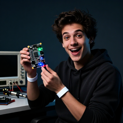
Breaking Taps, "Designing Silicon From Scratch". A maker who had "never done any chip design before" designs a small processor, tapes it out on a wafer.space run and brings it up on his bench. In his own words from the video:
- He had one month before the tape-out deadline, and wrote the design in Spade, a Rust-inspired hardware language ("If you want to learn to design a chip professionally, go learn Verilog").
- LibreLane turned the code into a layout, and wafer.space provides a Nix flake that sets the tools up.
- On a large rented server the whole build took about four hours, about two of them for the design-rule check.
- Turnaround at the foundry was "something like 3 to 4 months"; the dies came back as chip-on-board parts.
- He brought the chip up with a Raspberry Pi Pico and level shifters on breadboards, and flaky behaviour turned out to be a grounding problem, fixed with more ground jumpers.
- For a cheaper first step he points to Tiny Tapeout, which splits a die into small tiles.
2
2
What a slot costs
What a slot costs
Jupyter نوٹ بک لوڈ ہو رہی ہے…
3
3
What wafer.space is
What wafer.space is
wafer.space is a shared-wafer (multi-project) service. It collects many designs onto one GlobalFoundries wafer made on the GF180MCU process, a 180 nm mixed-signal process with five metal layers and 3.3 V and 5 V devices, and returns the dies to each designer.
Slot sizes for Run 3: 1x1 (3.93 × 5.12 mm), 0.5x1 (1.94 × 5.12 mm), 1x0.5 (3.93 × 2.53 mm) and 0.5x0.5 (1.94 × 2.53 mm), each with a 26 µm seal ring, and 1,000 dies per slot. Add-ons: chip-on-board packaging ($1.50 a die) or the whole undiced wafer ($2,000). The PDK is open; your design can be open or closed.
Run 3 dates as published: early bird until 30 September 2026, purchase deadline 9 December 2026, submission deadline 16 December 2026, parts shipped in Q2 2027. Run 1 has already delivered wire-bonded chip-on-board parts to its customers.
4
4
Where the chip comes from
Where the chip comes from
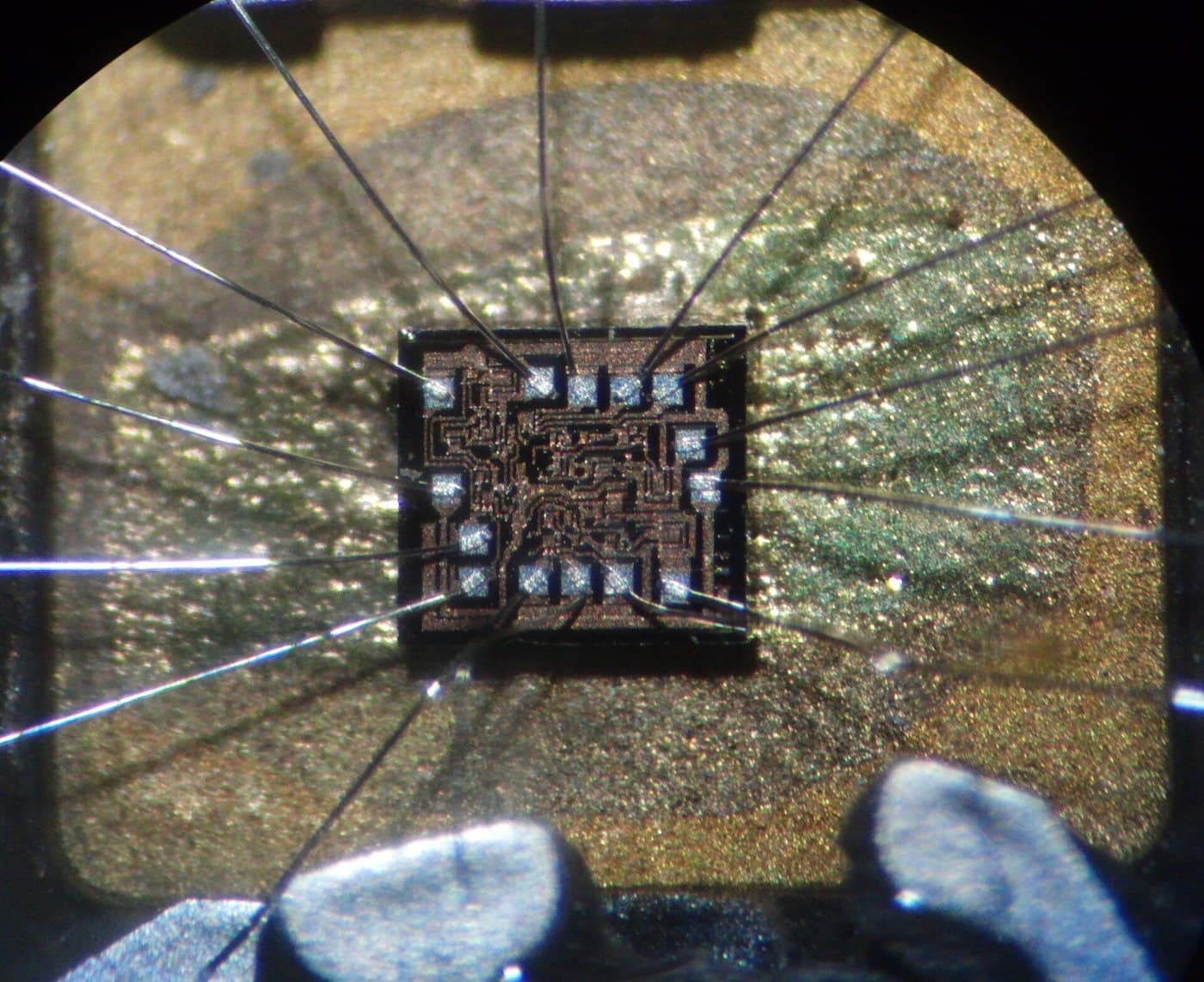
The embedded blueprint is the 1959 idea every chip on this wafer still follows: all the parts and the wiring made together, flat, on one piece of silicon.
5
5
What you need at home
What you need at home
**A computer.** LibreLane, the tool that turns your design into a layout, asks for at least a quad-core 2.0 GHz CPU and 8 GiB of RAM, and recommends a 6th-generation Intel Core or AMD Ryzen 1000-series CPU or later and 16 GiB. It is primarily supported on Ubuntu 22.04 and later; macOS 15 and later is supported, and Windows 10 (version 2004 and later) through the Windows Subsystem for Linux.
**The tools, through Nix.** The project template brings every tool in a Nix shell: LibreLane with Yosys, OpenROAD, Magic and KLayout, cocotb with Icarus Verilog for simulation, and GTKWave for waveforms. LibreLane's own warning: do not install Nix with apt, whose version is often out of date.
**A slot**, bought from wafer.space before the purchase deadline, and your finished layout submitted before the submission deadline.
**Time.** The design takes weeks; the foundry takes months. A long build also wants a fast machine: the maker in step 1 rented a large server to shorten his.
اس مرحلے کے لیے مواد:
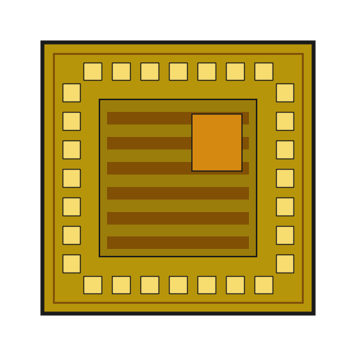 کسٹم ASIC ڈائی1000 ٹکڑے
درکار اوزار:
 ڈیسک ٹاپ کمپیوٹر
6
6
Install and run the template
Install and run the template
These commands are copied from the LibreLane installation guide and the wafer.space project template and precheck READMEs as they stood on 29 September 2026. They are documented steps, not a run recorded for this blueprint; follow the READMEs if they have changed.
first-chip.shbash
درکار اوزار:
ڈیسک ٹاپ کمپیوٹر7
7
Make it yours, within the template's rules
Make it yours, within the template's rules
Your logic goes in src/chip_core.sv, which receives the clock, the reset and the signals from the pads; chip_top.sv holds the pads, a chip ID QR code and the wafer.space logo. The template's rules, from its README:
- Keep the number of pads, so the bond pads stay where the default bonding expects them.
- Do not change the power or ground pads, or the chip no longer fits the default breakout board.
- You may change what the signal pads are: bidirectional, input-only or analog, set with NUM_INPUT and NUM_BIDIR.
The precheck then confirms one top cell, origin at (0,0), nothing above Metal5, the slot's dimensions and the pad openings for chip-on-board, and runs the density, antenna, Magic DRC and KLayout DRC checks.
8
8
What comes back
What comes back
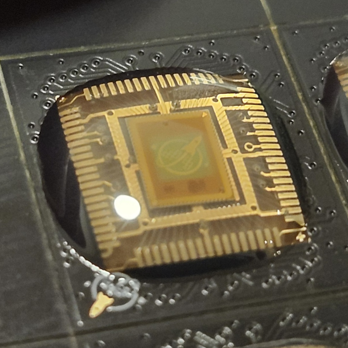
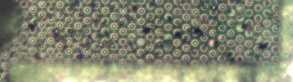
Each slot returns 1,000 dies. With the chip-on-board add-on, a die is glued to a small board, wire-bonded to its pads and covered in epoxy, as in this rung's photograph from Run 1.
For Run 1 the full-slot board is 14 × 16 mm, with the die's 74 bond pads following the Tiny Tapeout convention, all grounds tied together, and a 70-pin mezzanine connector underneath. wafer.space publishes example breakout motherboards and KiCad symbols for that connector, and notes that pinouts and connectors are specific to each run.
Wiring up that breakout board, and bringing up the chip on it, are the next rungs of this ladder.
9
9
A first chip that will not pass
A first chip that will not pass
First-chip troubleshooting.
Flow
Loading...
10
10
Sources and honest limits
Sources and honest limits
**Sources**, read 29 September 2026: wafer.space (home, prices, technology and FAQ pages); the wafer-space GitHub repositories gf180mcu-project-template, gf180mcu-precheck and chip-on-board-wire-bonded-pcbs (Apache-2.0); the LibreLane installation guide; and Breaking Taps, "Designing Silicon From Scratch" on YouTube.
**Honest limits.** The commands were not run for this blueprint: they are the maintainers' documented steps. Prices and dates are Run 3's as published and will change for later runs, and Run 1's board details are specific to that run. The build time and turnaround in step 1 are one maker's experience, not a promise. The photograph is wafer.space's own, from its chip-on-board repository.
مواد
1- 1000 ٹکڑےپلیس ہولڈر
درکار اوزار
1- پلیس ہولڈر
متعلقہ بلیو پرنٹ
یہ بلیو پرنٹ علم بانٹتے ہیں — تکنیک، مواد یا اصول


CC0 پبلک ڈومین
یہ بلیو پرنٹ CC0 کے تحت جاری کیا گیا ہے۔ آپ اجازت لیے بغیر اس کام کو نقل، ترمیم، تقسیم اور کسی بھی مقصد کے لیے استعمال کرنے کے لیے آزاد ہیں۔
میکر کی حمایت کریں ان کے بلیو پرنٹ کے ذریعے پروڈکٹس خرید کر جہاں وہ میکر کمیشن وینڈرز کی طرف سے مقرر، کماتے ہیں، یا اس بلیو پرنٹ کی نئی تکرار بنائیں اور آمدنی شیئر کرنے کے لیے اسے اپنے بلیو پرنٹ میں کنکشن کے طور پر شامل کریں۔