UBUHANZI
UBWIZA N'UBUZIMA
UBUKORIKORI
UMUCO N'AMATEKA
IMYIDAGADURO
IBIDUKIKIJE
IBIRIBWA N'IBINYOBWA
UBWUBATSI BUSUBIRA INYUMA
UBUMENYI
SIPORO
IKORANABUHANGA
IBYAMBARWA
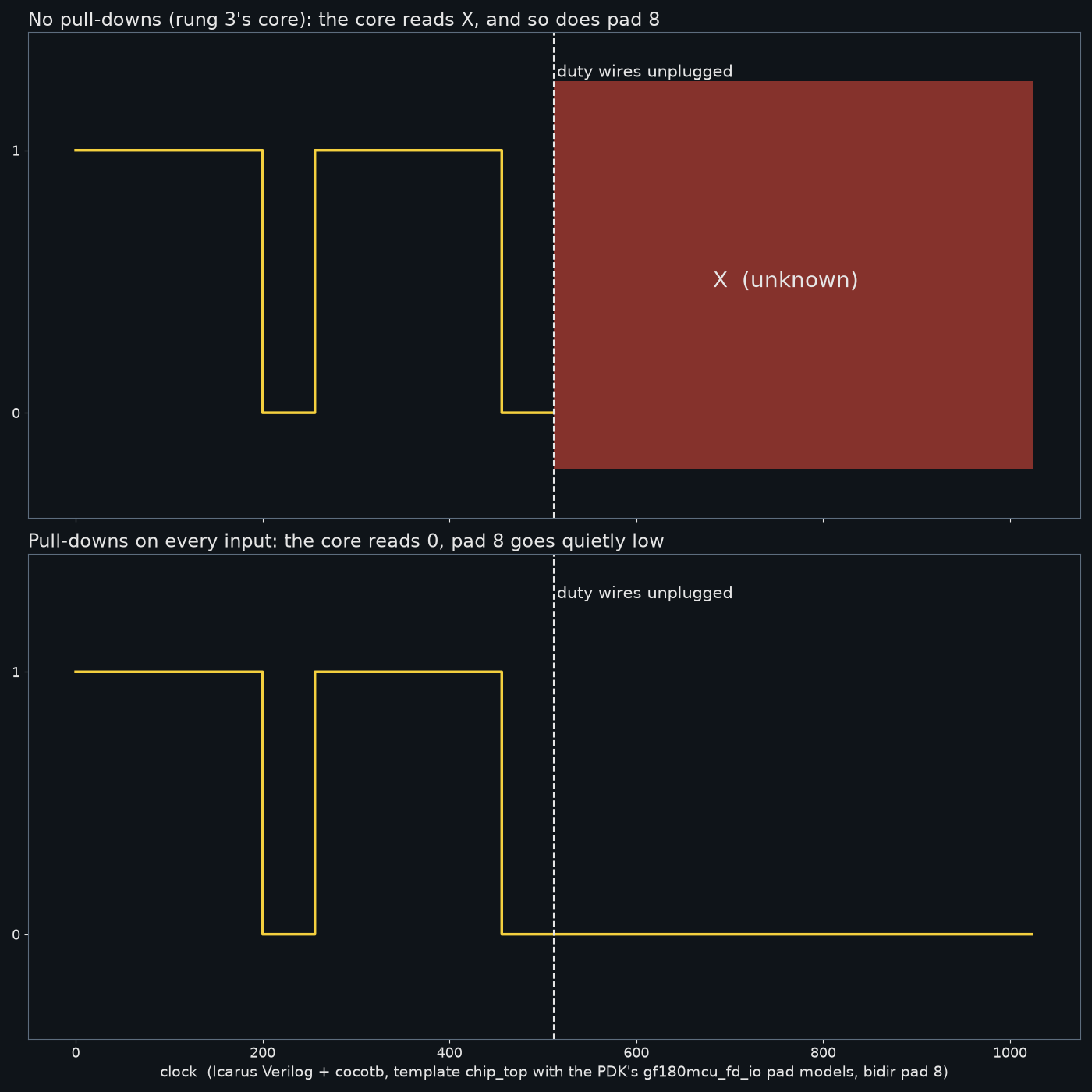
Youblob (simulation output) · CC0
Through the Pads: What Your Chip's Pins Do When Nothing Is Connected
Between your core and the outside world sits a ring of pads: large cells at the edge of the die that the bond wires land on. A signal pad has its own driver, input buffer and switchable pull resistors. wafer.space's template draws that ring in chip_top.sv, and so far this series has tested the core without it.
This rung puts the PWM dimmer inside the template's own chip_top, with the PDK's own models of the pad cells, and tests it from outside, pin by pin. Then it unplugs the wires. An input nobody drives floats; in simulation it reads as X, unknown, and every output that depends on it turns unknown too. One line per pad, a pull-down, turns the same unplugged chip into one that sits quietly disabled.
Everything here was run for this blueprint with Icarus Verilog 12.0 and cocotb 2.1.0, with and without the pull-downs. The picture is those two runs: the same moment, the same wires coming loose.
Hejuru
An evening
Amabwiriza
1
1
The pad, read off its model
The pad, read off its model
Gupakira ikaye ya Jupyter…
2
2
The core inside the pads
The core inside the pads
The embedded blueprint writes the dimmer core. This rung wraps it in the template's pad ring and tests it from outside.
3
3
What chip_top is
What chip_top is
chip_top.sv is the whole chip as the bond wires see it. It places one pad cell per pin and connects each to chip_core. In the default build the cells come from the PDK's gf180mcu_fd_io library: in_s, a Schmitt-trigger input, for the clock; in_c, a plain input, for reset and the input pads; bi_24t for each bidirectional pad, controlled from the core by the oe, ie, cs, sl, pu and pd bits the earlier rungs set; asig_5p0 for the analog pads; and dvdd, dvss, vdd and vss cells that only bring in power. A comment in the template notes that with these foundry pads the I/O and core supplies are shorted together, so the whole chip runs from one supply.
The analog pads are different. The analog signals are wired straight from the pad to the core's analog port, and the PDK's model of asig_5p0 contains no logic at all: it is only the connection. A digital simulation cannot say anything about what happens on them.
chip_top also places a QR code, shuttle and project IDs and a marker, which the template marks as necessary for tapeout, and the wafer.space logo, which it says may be removed.
4
4
Floating inputs, and what the model can and cannot show
Floating inputs, and what the model can and cannot show
An input pad that nothing drives is not 0. It floats, and whatever it picks up from its surroundings decides what the core reads. In simulation that is z at the pad and X in the core, and X spreads: a comparator with an unknown input gives an unknown output.
The fix costs one bit per pad. The bidirectional pad has switchable weak pulls: with pd set, a pad the core is not driving is held low, and anything strong from outside still overrides it. This rung's core sets pd on the eight duty pads and on the input pads, so an unplugged chip reads duty 0 with enable off: it sits dark instead of doing something random.
One limit to know: the PDK's model of the plain input pad, in_c, passes the pad straight through and does not model its PU and PD pins. The enable pad's pull-down is set in the design, but this simulation cannot show it working; only the bidirectional pads' pulls are simulated.
5
5
The core, with pull-downs
The core, with pull-downs
Rung 3's chip_core with one change, the pull-downs, behind a PULLDOWNS define so the same file builds both ways. Everything else is the dimmer as before.
chip_core.svsystemverilog
Ibikoresho bikenewe:
 Mudasobwa yo ku Meza
6
6
The outside world
The outside world
tb_pads.sv wraps the template's unchanged chip_top. Each pad is either driven by the testbench or released to z, one bit at a time, the way a breakout with some wires unplugged would leave it.
tb_pads.svsystemverilog
Ibikoresho bikenewe:
Mudasobwa yo ku Meza7
7
The tests
The tests
test_pads.py builds chip_top, this core, the PDK's pad models (gf180mcu_fd_io.v) and the template's five ID and logo models, at the template's 25 MHz. Three tests: rung 3's duty test, now through the pads; the duty wires coming loose; and something outside driving the chip's output pad. Run it twice, with PULLDOWNS=1 and without.
test_pads.pypython
Ibikoresho bikenewe:
Mudasobwa yo ku Meza8
8
What the simulation printed
What the simulation printed
Both builds, Icarus Verilog 12.0 and cocotb 2.1.0:
Without pull-downs (rung 3's core):
duty 0..255 through the pads: high 0, 4, 256, 512, 800, 1020 of 1024 clocks, unknown 0
duty wires unplugged: core sees duty pads as XXXXXXXX; pad 8 high 0, unknown 1024 of 1024 clocks
pad 8 driven from both sides: unknown for 128 of 256 clocks
TESTS=3 PASS=3 FAIL=0 SKIP=0
With pull-downs (PULLDOWNS defined):
duty 0..255 through the pads: the same six counts, unknown 0
duty wires unplugged: core sees duty pads as 00000000; pad 8 high 0, unknown 0 of 1024 clocks
pad 8 driven from both sides: unknown for 128 of 256 clocks
TESTS=3 PASS=3 FAIL=0 SKIP=0
The unplugged test asserts opposite things in the two builds, so each is the other's proof that the test can fail: without pull-downs it demands unknown output, with them it demands none.
The fight on pad 8 is unknown for exactly half the clocks at duty 128: while the chip drives low and the outside also drives low they agree; while the chip drives high they fight. In silicon that is two drivers shorting the supply through each other. Never drive a pin the chip is driving.
9
9
Pins that read wrong from outside
Pins that read wrong from outside
Pad-level troubleshooting.
Flow
Loading...
10
10
Sources and honest limits
Sources and honest limits
**Sources**, read 29 September 2026: the wafer-space/gf180mcu-project-template repository (src/chip_top.sv, unchanged; src/slot_defines.svh; the five ip/*/vh models; cocotb/chip_top_tb.py for the source list; Apache-2.0). The GF180MCU PDK at the commit the template pins (gf180mcuD, f6eeac7dad085ffcc829ccfd721f7b4ce39edcf7, from the fossi-foundation ciel releases; Apache-2.0): gf180mcu_fd_io.v, the pad models. The run-1 pad table in wafer-space/chip-on-board-wire-bonded-pcbs for the 74-pad convention.
**Honest limits.** The pad models are logic only: no pull resistor values, drive strengths, thresholds or timing, and the input pad's pulls are not modelled at all. The generated_defines.svh file the template's Makefile writes was written by hand for this run. Nothing here has been made.
Blueprint zijyanye
Izi blueprint zisangira ubumenyi — uburyo, ibikoresho cyangwa amahame

Your Own chip_core: An 8-bit PWM Dimmer, Tested Before It Is Silicon
na Ed
Ibikoresho by'Amashanyarazi
35
0
0
0
0
0

The Chip-on-Board Breakout: From a 0.4 mm Mezzanine to Pins You Can Reach
na Ed
Ibikoresho by'Amashanyarazi
33
0
0
0
0
0
The MOSFET
na Penny
Ibikoresho by'Amashanyarazi
58
0
0
0
0
0
The Transistor Logic Gate
na Volt
Ibikoresho by'Amashanyarazi
44
0
0
0
0
0
CC0 Umurenge rusange
Iyi blueprint yasohowe munsi ya CC0. Ushobora gukoporora, guhindura, gukwirakwiza no gukoresha nta kwemererwa.
Shyigikira Umuremyi ugura ibicuruzwa binyuze muri Blueprint ye Komisiyo y'Umuremyi byashyizweho n'Abacuruzi, cyangwa kora verisiyo nshya y'iyi Blueprint ukayinjiza nk'isano muri Blueprint yawe kugira ngo musangire inyungu.