التعاون
فنون
الجمال والعناية
حِرَف
الثقافة والتاريخ
ترفيه
البيئة
الطعام والمشروبات
الهندسة العكسية
العلوم
رياضة
التقنية
الأجهزة القابلة للارتداء
الذاكرة المدمجة على الشريحة: ضوء يتنفس مخزَّن في ذاكرة الشريحة نفسها
English
Youblob (simulation output) · CC0
Ed

أنشأه

Ed

29. سبتمبر 2026FI
49
0
0
0
0

الذاكرة المدمجة على الشريحة: ضوء يتنفس مخزَّن في ذاكرة الشريحة نفسها

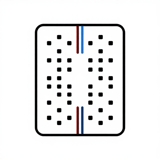
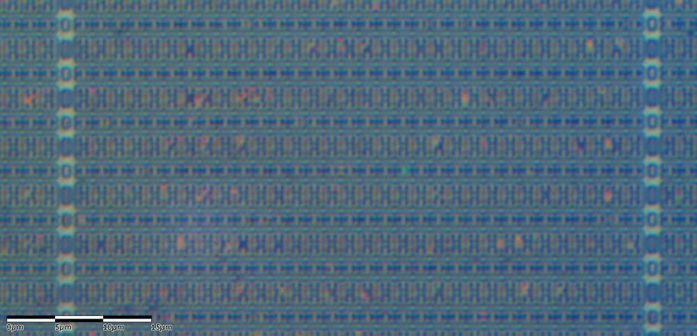
يأتي قالب wafer.space مع ماكروين من نوع SRAM في تصميمه التجريبي، بحجم 512 بايت لكل منهما، ويتركهما مُعطّلين. الماكرو كتلة ذاكرة جاهزة من PDK: 4096 خلية ذاكرة ثابتة، رُسمت مرة واحدة مع دارة فك العناوين ودوائر القراءة، وتُوضع كاملةً بدلاً من بنائها من البوابات. تُفعّل هذه المرحلة أحدهما. يُشغّل المُعتِم (dimmer) من المرحلة السابقة الآن نمطاً: يكتب متحكم دقيق 256 بايت إلى الشريحة عبر نقاط توصيلها مرة واحدة، ومن ثم تقرأها الشريحة بنفسها بايتاً واحداً في كل خطوة، لتُستخدم كسطوع لضوء يتنفس ببطء. شُغِّل النواة وبيئة اختبارها لهذا المخطط باستخدام Icarus Verilog 12.0 وcocotb 2.1.0 ونموذج المحاكاة الخاص بـ PDK لماكرو SRAM: تبع الخرج الجدول المخزَّن لمدة 600 دورة PWM. الصورة هي الخرج الخاص بتلك المحاكاة، عمود واحد لكل دورة. نُفّذ الكود ESP32 الذي يُحمِّل الجدول لهذا المخطط؛ ولا توجد شريحة فعلية بعد لتشغيله عليها.
متقدم
مساءٌ، والشريحة

التعليمات

1

النمط والتوقيت والحجم

جارٍ تحميل دفتر Jupyter…
2

ما يمثله كل بت من البتات الـ 4,096

يوضح المخطط المضمّن كيف يحتفظ بت واحد من الذاكرة الساكنة بحالته: حلقة مكوّنة من مقلوبين (عاكسين). والماكرو في هذه المرحلة هو 4,096 بت من الذاكرة الساكنة في مصفوفة واحدة.
3

مسامير الماكرو، وثلاثة أشياء يقولها نموذجه

يحتوي gf180mcu_fd_ip_sram__sram512x8m8wm1 على 512 بايت. أطرافه: CLK؛ A، عنوان من 9 بتات؛ D، البايت المراد كتابته؛ Q، البايت المقروء. جميع عناصر التحكم الثلاثة فعّالة عند LOW. CEN عند 0 يُشغّل الذاكرة. GWEN عند 0 يجعل حافة الساعة عملية كتابة، وعند 1 عملية قراءة. WEN يحتوي على بت واحد لكل بت بيانات، والقيمة 0 تسمح بكتابة ذلك البت، لذا قد تغيّر عملية الكتابة بعض بتات البايت وتترك الباقي دون تغيير. وبقراءة نموذج المحاكاة الخاص بـ PDK يتبين ثلاثة أمور جديرة بالمعرفة. أولاً، لا تعمل الذاكرة إلا بعد أن ينتقل CEN من 1 إلى 0؛ وإلا يطبع النموذج “CEN is not reset, memory is not operational”، لذا تُبقي النواة CEN على 1 طوال فترة إعادة الضبط ثم تخفضه بعد ذلك. ثانياً، تعطي القراءة mem[A] على Q مباشرةً بعد حافة الساعة التي أخذت عينة من A، لذا تكون البيانات جاهزة بعد دورة ساعة واحدة. ثالثاً، يبدأ النموذج بكل البايتات مساوية للصفر. أما الشريحة الحقيقية فلا تفعل ذلك: إذ إن SRAM يُشغَّل وهو يحمل ما استقرت عليه كل خلية، لذا يجب أن يكتب التصميم قبل أن يقرأ. يربط المثال الخاص بالقالب CEN بالقيمة 1، فيبقى الماكرو الاثنان مغلقين. وتشير ملفات التوقيت الخاصة به إلى أن الحد الأدنى لدورة الساعة للماكرو هو 6.6 ns عند زاوية التشغيل النموذجية 5 V، و18.3 ns عند زاوية 3.0 V البطيئة و125 °C، وكلاهما أقل بكثير من 40 ns الخاصة بالقالب.
4

The core

src/chip_core.sv for the pattern player, with the template's port list unchanged plus one parameter, HOLD_LOG2. Input pad 0 enables, pad 1 selects LOAD mode, pad 2 is the write strobe; bidirectional pads 0 to 7 carry the byte, pad 8 the PWM. The LOAD and strobe pads are passed through two flip-flops before use, a synchroniser: they change whenever the outside world likes, not in step with the chip's clock, and a flip-flop caught mid-change can hover between 0 and 1 for a while. In play mode, each time HOLD_LOG2 periods have passed, the byte the SRAM has been reading becomes the new duty and the address moves on.
chip_core.svsystemverilog
// SPDX-License-Identifier: Apache-2.0
// Youblob silicon rung 5: the PWM dimmer plays a brightness pattern stored in the on-chip SRAM macro.
// Port list unchanged from wafer-space/gf180mcu-project-template src/chip_core.sv.

`default_nettype none

module chip_core #(
    parameter NUM_INPUT_PADS,
    parameter NUM_BIDIR_PADS,
    parameter NUM_ANALOG_PADS,
    parameter HOLD_LOG2 = 9        // each table entry lasts 2**HOLD_LOG2 PWM periods
    )(
    `ifdef USE_POWER_PINS
    inout  wire VDD,
    inout  wire VSS,
    `endif

    input  wire clk,       // clock
    input  wire rst_n,     // reset (active low)

    input  wire [NUM_INPUT_PADS-1:0] input_in,   // Input value
    output wire [NUM_INPUT_PADS-1:0] input_pu,   // Pull-up
    output wire [NUM_INPUT_PADS-1:0] input_pd,   // Pull-down

    input  wire [NUM_BIDIR_PADS-1:0] bidir_in,   // Input value
    output wire [NUM_BIDIR_PADS-1:0] bidir_out,  // Output value
    output wire [NUM_BIDIR_PADS-1:0] bidir_oe,   // Output enable
    output wire [NUM_BIDIR_PADS-1:0] bidir_cs,   // Input type (0=CMOS Buffer, 1=Schmitt Trigger)
    output wire [NUM_BIDIR_PADS-1:0] bidir_sl,   // Slew rate (0=fast, 1=slow)
    output wire [NUM_BIDIR_PADS-1:0] bidir_ie,   // Input enable
    output wire [NUM_BIDIR_PADS-1:0] bidir_pu,   // Pull-up
    output wire [NUM_BIDIR_PADS-1:0] bidir_pd,   // Pull-down

    inout  wire [NUM_ANALOG_PADS-1:0] analog  // Analog
);

    // Input pad 0: enable.  Input pad 1: LOAD mode.  Input pad 2: write strobe.
    // Bidir pads 0..7: the byte to store while loading.  Bidir pad 8: the PWM output.
    localparam DUTY_W = 8;
    localparam PWM_PAD = 8;

    assign input_pu = '0;
    assign input_pd = '0;
    assign bidir_oe = {{(NUM_BIDIR_PADS-DUTY_W){1'b1}}, {DUTY_W{1'b0}}};
    assign bidir_ie = ~bidir_oe;
    assign bidir_cs = {{(NUM_BIDIR_PADS-DUTY_W){1'b0}}, {DUTY_W{1'b1}}};
    assign bidir_sl = '0;
    assign bidir_pu = '0;
    assign bidir_pd = '0;

    wire enable = input_in[0];
    wire [DUTY_W-1:0] data_in = bidir_in[DUTY_W-1:0];

    // The mode and strobe pads change whenever the outside world likes, not in step with clk:
    // two flip-flops in a row (a synchroniser) before anything uses them.
    logic [1:0] load_s;
    logic [2:0] strobe_s;
    always_ff @(posedge clk) begin
        load_s   <= {load_s[0], input_in[1]};
        strobe_s <= {strobe_s[1:0], input_in[2]};
    end
    logic load_was;
    wire load        = load_s[1];
    wire load_start  = load & ~load_was;
    wire strobe_rise = strobe_s[1] & ~strobe_s[2];
    always_ff @(posedge clk) load_was <= load;

    // The SRAM wants its chip enable (CEN, active LOW) to go 1 -> 0 before it works:
    // hold it at 1 through reset, then 0.
    logic cen;
    always_ff @(posedge clk) cen <= !rst_n;

    // PWM counter and the "hold" counter that decides when to step to the next table entry.
    logic [DUTY_W-1:0] count;
    logic [HOLD_LOG2:0] hold;                   // one bit wider so HOLD_LOG2 = 0 still works
    wire period_end = (count == '1);
    localparam logic [HOLD_LOG2:0] HOLD_MASK = (1 << HOLD_LOG2) - 1;   // 0 when HOLD_LOG2 = 0
    wire step = period_end && ((hold & HOLD_MASK) == HOLD_MASK);

    logic [DUTY_W-1:0] addr;
    logic [DUTY_W-1:0] duty;
    wire  [DUTY_W-1:0] q;                       // SRAM read data: mem[addr], one clock after addr

    always_ff @(posedge clk) begin
        if (!rst_n) begin
            count <= '0;  hold <= '0;  addr <= '0;  duty <= '0;
        end else if (load) begin
            count <= '0;  hold <= '0;  duty <= '0;
            if (load_start)       addr <= '0;       // every load starts at entry 0
            else if (strobe_rise) addr <= addr + 1'b1;
        end else if (enable) begin
            count <= count + 1'b1;
            if (period_end) hold <= hold + 1'b1;
            if (step) begin
                duty <= q;                          // the entry that was being read
                addr <= addr + 1'b1;                // and move on to the next
            end
        end
    end

    `gf180mcu_xxx_ip_sram__sram512x8m8wm1 sram_0 (
        `ifdef USE_POWER_PINS
        .VDD  (VDD),
        .VSS  (VSS),
        `endif
        .CLK  (clk),
        .CEN  (cen),                                   // active low: 0 = on
        .GWEN (~(load && strobe_rise)),                // active low: 0 = write this clock
        .WEN  (8'b0),                                  // active low, per bit: write all eight
        .A    ({1'b0, addr}),                          // 256 of the 512 bytes
        .D    (data_in),
        .Q    (q)
    );

    logic pwm;
    always_ff @(posedge clk) begin
        if (!rst_n) pwm <= 1'b0;
        else        pwm <= enable && !load && (count < duty);
    end

    logic [NUM_BIDIR_PADS-1:0] out;
    always_comb begin
        out = '0;
        out[PWM_PAD] = pwm;
    end
    assign bidir_out = out;

    // Inputs this design does not read (keeps lint quiet, as the template does with _unused).
    logic _unused;
    assign _unused = &{1'b0, input_in[NUM_INPUT_PADS-1:3], bidir_in[NUM_BIDIR_PADS-1:DUTY_W], hold[HOLD_LOG2]};

endmodule

`default_nettype wire

الأدوات المطلوبة:

حاسوب مكتبيحاسوب مكتبي
5

The test

test_pattern.py builds the core with the PDK's SRAM model, gf180mcu_fd_ip_sram__sram512x8m8wm1.v, at the template's 25 MHz and with HOLD_LOG2 = 0 so the whole table plays in 256 periods. It loads the table through the pads the way the ESP32 will, then counts the high clocks in each of 600 PWM periods and requires them to follow the table from exactly one starting point. A second test loads again and checks the new pattern replaced the old.
test_pattern.pypython
# SPDX-License-Identifier: Apache-2.0
# cocotb testbench for the SRAM pattern player, with the PDK's own SRAM simulation model
# (gf180mcu_fd_ip_sram__sram512x8m8wm1, gf180mcuD, the commit the template pins).
import math
import os
from pathlib import Path

import cocotb
from cocotb.clock import Clock
from cocotb.triggers import ClockCycles, FallingEdge, RisingEdge
from cocotb_tools.runner import get_runner

PWM_PAD = 8
EN, LOAD, STROBE = 1, 2, 4                      # input pad bits
SRAM = Path(os.getenv("PDK_ROOT", "pdk")) / "gf180mcuD" / "libs.ref" / "gf180mcu_fd_ip_sram" / "verilog"


def breathing_table(n=256, gamma=2.2):
    """One slow breath: a raised sine, gamma-corrected so equal steps LOOK equal to the eye."""
    return [round(255 * ((1 - math.cos(2 * math.pi * i / n)) / 2) ** gamma) for i in range(n)]


async def start(dut):
    cocotb.start_soon(Clock(dut.clk, 40, unit="ns").start())   # 25 MHz, the template's CLOCK_PERIOD
    dut.input_in.value = 0
    dut.bidir_in.value = 0
    dut.rst_n.value = 0
    await ClockCycles(dut.clk, 5)
    dut.rst_n.value = 1
    await ClockCycles(dut.clk, 2)


async def load(dut, table):
    """What a microcontroller on the breakout does: LOAD high, then per byte set the data pads,
    raise the strobe, wait, lower it. The chip synchronises the strobe, so hold each for 4 clocks."""
    dut.input_in.value = LOAD
    await ClockCycles(dut.clk, 4)
    for b in table:
        dut.bidir_in.value = b
        await ClockCycles(dut.clk, 1)
        dut.input_in.value = LOAD | STROBE
        await ClockCycles(dut.clk, 4)
        dut.input_in.value = LOAD
        await ClockCycles(dut.clk, 4)
    dut.input_in.value = 0
    await ClockCycles(dut.clk, 4)


async def highs_per_period(dut, periods):
    """High clocks in each PWM period, counted from the core's own count = 0."""
    while int(dut.count.value) != 0:
        await RisingEdge(dut.clk)
    out = []
    for _ in range(periods):
        n = 0
        for _ in range(256):
            await FallingEdge(dut.clk)
            n += int(dut.bidir_out.value[PWM_PAD])
        out.append(n)
    return out


@cocotb.test()
async def test_plays_the_table(dut):
    """Load a 256-entry breathing table, play it: each period's high time is the next entry."""
    table = breathing_table()
    await start(dut)
    await load(dut, table)
    dut.input_in.value = EN
    got = await highs_per_period(dut, 600)
    # the output starts part-way through the table; find where, then demand every period match
    fits = [off for off in range(256) if all(got[j] == table[(j + off) % 256] for j in range(2, 600))]
    dut._log.info(f"first periods {got[:8]}, table aligns at offset {fits}")
    Path(__file__).resolve().parent.joinpath("pattern_trace.csv").write_text("\n".join(map(str, got)))
    assert len(fits) == 1, f"the output does not follow the table (offsets that fit: {fits})"


@cocotb.test()
async def test_reload(dut):
    """Loading again replaces the pattern: a flat 64 gives 64 high clocks every period."""
    await start(dut)
    await load(dut, breathing_table())
    await load(dut, [64] * 256)
    dut.input_in.value = EN
    got = await highs_per_period(dut, 40)
    assert all(g == 64 for g in got[2:]), got


def test_runner():
    here = Path(__file__).resolve().parent
    defines = {"gf180mcu_xxx_ip_sram__sram512x8m8wm1": "gf180mcu_fd_ip_sram__sram512x8m8wm1"}
    runner = get_runner("icarus")
    runner.build(
        sources=[SRAM / "gf180mcu_fd_ip_sram__sram512x8m8wm1.v", here / "chip_core.sv"],
        hdl_toplevel="chip_core",
        parameters={"NUM_INPUT_PADS": 4, "NUM_BIDIR_PADS": 38, "NUM_ANALOG_PADS": 4, "HOLD_LOG2": 0},
        defines=defines,
        build_args=["-g2012"],
        timescale=("1ns", "1ps"),
        always=True,
    )
    runner.test(hdl_toplevel="chip_core", test_module="test_pattern")


if __name__ == "__main__":
    test_runner()

الأدوات المطلوبة:

حاسوب مكتبيحاسوب مكتبي
6

ما طبعته المحاكاة

شغّل هذا المخطط باستخدام Icarus Verilog 12.0 وcocotb 2.1.0: -------- MESSAGE: CEN أُعيد ضبطه للتو، والذاكرة تعمل --------- test_pattern.test_plays_the_table PASS (600 دورة، يتطابق الجدول عند إزاحة واحدة بالضبط) test_pattern.test_reload PASS TESTS=2 PASS=2 FAIL=0 SKIP=0 لإثبات أن الاختبار يمكن أن يفشل، تم تغيير WEN من 8'b0 إلى 8'hFF، وهو الخطأ الكلاسيكي مع دبوس نشط عند الانخفاض: كل بت مُقنّع، ولا شيء مكتوب، وجدول من الأصفار. فشل الاختباران، وأُعيد النواة إلى حالتها الأصلية. السطر الأول هو رسالة نموذج SRAM الخاصة: خفّضت النواة CEN بعد إعادة الضبط، كما يشترط النموذج.
7

Load it from an ESP32

Once the chip is on its breakout board, this sketch writes the table. Eight GPIOs carry the byte, three more drive LOAD, the strobe and enable, and an LED with a 330 ohm resistor from pad 8 to ground shows the breath. Each level is held for 1 microsecond, 25 of the chip's clocks, so the synchroniser always sees it. The sketch then does nothing: the pattern lives in the chip. It is lost when the chip loses power, so send r over serial to load it again. The ESP32 is a 3.3 V part and its inputs are not 5 V tolerant. The sketch only drives the chip and never reads from it. The template's default libraries are the 5 V ones; before you connect, check in the I/O library's documentation that 3.3 V is a valid logic high for your chip's inputs, or build with the 3.3 V libraries, as the template's README shows. The sketch compiles for the ESP32 with the Arduino ESP32 core 3.3.12; it has not been run, because the chip does not exist yet.
load_pattern.inocpp
// SPDX-License-Identifier: Apache-2.0
// Load a breathing pattern into your chip's SRAM through its pads, then let the chip play it.
// Youblob silicon rung 5. The chip does the playing; this board only writes 256 bytes once.
//
// Wiring (ESP32 GPIO -> chip pad on your breakout):
//   D0..D7  GPIO 13,14,18,19,21,22,23,25 -> bidir[0..7]
//   LOAD    GPIO 26 -> input[1]
//   STROBE  GPIO 27 -> input[2]
//   EN      GPIO 32 -> input[0]
//   and a common ground. The chip's bidir[8] drives an LED through 330 ohm to ground.
// The ESP32 is a 3.3 V part: run the chip's I/O at 3.3 V, or put a level shifter between them.

#include <math.h>

const int DATA_PINS[8] = {13, 14, 18, 19, 21, 22, 23, 25};
const int PIN_LOAD = 26, PIN_STROBE = 27, PIN_EN = 32;

// The chip passes LOAD and STROBE through a two-flip-flop synchroniser and looks for the strobe's
// rising edge, so every level has to last a few of ITS clocks. 1 us is 25 clocks at 25 MHz.
const unsigned HOLD_US = 1;

uint8_t table[256];

void makeBreathingTable() {
  // a raised sine, gamma-corrected (2.2) so the brightness steps look even to the eye
  for (int i = 0; i < 256; i++) {
    float s = (1.0f - cosf(2.0f * PI * i / 256.0f)) / 2.0f;
    table[i] = (uint8_t)lroundf(255.0f * powf(s, 2.2f));
  }
}

void putByte(uint8_t b) {
  for (int bit = 0; bit < 8; bit++) digitalWrite(DATA_PINS[bit], (b >> bit) & 1);
  delayMicroseconds(HOLD_US);            // data settles before the strobe
  digitalWrite(PIN_STROBE, HIGH);        // the chip writes on the strobe's rising edge...
  delayMicroseconds(HOLD_US);            // ...a few of its clocks later, so hold the data
  digitalWrite(PIN_STROBE, LOW);
  delayMicroseconds(HOLD_US);
}

void loadTable() {
  digitalWrite(PIN_EN, LOW);
  digitalWrite(PIN_LOAD, HIGH);          // entering LOAD resets the chip's address to 0
  delayMicroseconds(HOLD_US);
  for (int i = 0; i < 256; i++) putByte(table[i]);
  digitalWrite(PIN_LOAD, LOW);
  delayMicroseconds(HOLD_US);
}

void setup() {
  Serial.begin(115200);
  for (int bit = 0; bit < 8; bit++) pinMode(DATA_PINS[bit], OUTPUT);
  pinMode(PIN_LOAD, OUTPUT);
  pinMode(PIN_STROBE, OUTPUT);
  pinMode(PIN_EN, OUTPUT);
  digitalWrite(PIN_STROBE, LOW);

  makeBreathingTable();
  loadTable();
  digitalWrite(PIN_EN, HIGH);            // play
  Serial.println("pattern loaded; the chip is playing it on its own");
  Serial.printf("table[0]=%u table[64]=%u table[128]=%u\n", table[0], table[64], table[128]);
}

void loop() {
  // Nothing to do: the pattern lives in the chip's SRAM now.
  // Send 'r' over serial to load it again (the SRAM loses it when the chip loses power).
  if (Serial.available() && Serial.read() == 'r') {
    loadTable();
    digitalWrite(PIN_EN, HIGH);
    Serial.println("reloaded");
  }
}

المواد لهذه الخطوة:

رقاقة ASIC مخصصةرقاقة ASIC مخصصة1 قطعة
لوح دارة مطبوعةلوح دارة مطبوعة1 قطعة
مصباح LED قياس 5 مممصباح LED قياس 5 مم1 قطعة
مقاومة 330 أوممقاومة 330 أوم1 قطعة

الأدوات المطلوبة:

لوحة تطوير ESP32لوحة تطوير ESP32
لوحة تجاربلوحة تجارب
أسلاك توصيلأسلاك توصيل
حاسوب مكتبيحاسوب مكتبي
8

نمط لا يتم حفظه أو لا يتم تشغيله

استكشاف أخطاء نمط SRAM وإصلاحها.

Flow

Loading...
9

المصادر والحدود الصريحة

**المصادر**، تمت قراءتها في 29 سبتمبر 2026: GF180MCU PDK عند الالتزام (commit) الذي يثبّته القالب، gf180mcuD، f6eeac7dad085ffcc829ccfd721f7b4ce39edcf7، من إصدارات fossi-foundation ciel؛ ترخيص Apache-2.0): نموذج SRAM gf180mcu_fd_ip_sram__sram512x8m8wm1.v، وLEF الخاص به للمخطط، وملفات توقيته لأدنى فترة ساعة؛ ملف توقيت مكتبة الخلايا القياسية لمساحة الفليب فلوب. مستودع wafer-space/gf180mcu-project-template (src/chip_core.sv، src/chip_top.sv، README.md، librelane/config.yaml؛ ترخيص Apache-2.0). **حدود صادقة.** تجري المحاكاة على مستوى chip_core باستخدام نموذج SRAM الخاص به، لكن دون حلقة الوصلات (pad ring) أو التركيب (synthesis) أو التخطيط (layout)، ولا تحسم فحوصات التوقيت الخاصة بالنموذج أي شيء هنا. تم تجميع مخطط ESP32 ولم يُشغَّل. كان HOLD_LOG2 يساوي 0 في الاختبار حتى ينتهي؛ أما الشريحة فكانت ستستخدم 9، أي نفسًا مدته نحو 1.3 ثانية.

المواد

4

الأدوات المطلوبة

4

CC0 ملكية عامة

هذا المخطط مُصدر بموجب CC0. يحق لك نسخه وتعديله وتوزيعه واستخدامه لأي غرض، دون طلب إذن.

ادعم الصانع بشراء منتجات عبر مخططه حيث يكسب عمولة الصانع يحددها البائعون، أو أنشئ نسخة جديدة من هذا المخطط وضمّنه كرابط في مخططك لمشاركة الإيرادات.

النقاش

(0)

تسجيل الدخول للمشاركة في النقاش

جارٍ تحميل التعليقات...