МИСТЕЦТВО
КРАСА ТА ЗДОРОВ'Я
РЕМЕСЛО
КУЛЬТУРА ТА ІСТОРІЯ
РОЗВАГИ
СЕРЕДОВИЩЕ
ЇЖА ТА НАПІЇ
ЗБОРНА ІНЖЕНЕРІЯ
НАУК
СПОРТ
ТЕХНОЛОГІЯ
НОСИМО
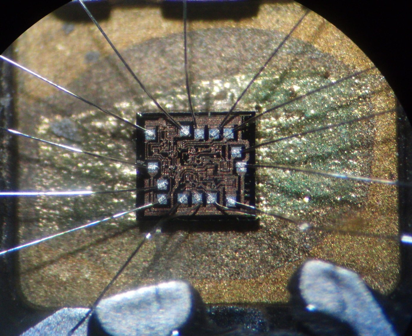


The Integrated Circuit — Noyce's Monolithic Planar
This is a sibling of `integrated-circuit-kilby`, not a replacement for it. Same goal — many components in one piece of semiconductor. Completely different means, and a completely different cost structure. Read that one first; this one only makes sense as a comparison.
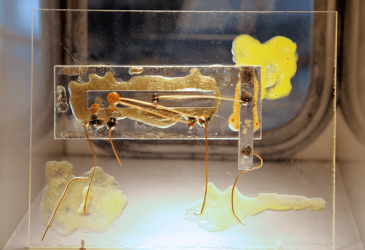
Kilby proved in September 1958 that components could be FORMED together. He connected them with gold wires bonded on by hand, and that left the harder half of the problem untouched: the wires scale one for one with the components, so a thousand-component chip needs a thousand hand-placed connections, which is the tyranny of numbers with extra steps.
Robert Noyce, at Fairchild, had something Kilby did not: Jean Hoerni's planar process, four months old and sitting in the same building. Hoerni had left the oxide on the wafer to seal the junctions, and in doing so had produced a FLAT, INSULATING surface over the whole device.
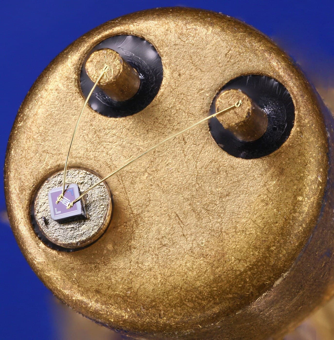
Noyce's notebook entry of January 1959 makes the connection in a few lines. If the surface is flat and insulating, you can evaporate a film of aluminium over the entire wafer. If you can evaporate a film, you can pattern it with photolithography — which the plant was already doing to define the diffusion windows. And a photolithographic pattern costs the same whether it contains one wire or ten thousand, because the light exposes them all at once.
That is the whole invention: interconnect that is PRINTED rather than PLACED. It converts the labour of wiring from proportional to the component count into independent of it, and everything about the economics of electronics for the next sixty years follows from that one change.
He filed in July 1959. The two patents collided, litigation ran a decade, and the companies cross-licensed in 1966. The industry built on Noyce's method and paid both.
You will build the same logic function three ways — discrete, hybrid, monolithic — and count the labour in each, which is the only way to feel why the third one won.
Просунутий
6 hours
Інструкції
1
1
The four things that had to be true at once
The four things that had to be true at once
Noyce's insight was not a device or a material. It was noticing that four separate developments, all present at Fairchild in early 1959, together permitted something none of them permitted alone. That is worth laying out explicitly, because it is a good example of an invention that is a recombination rather than a discovery.
ONE: the planar process gave a flat surface. Hoerni left the oxide on to seal junctions; the side effect was that the wafer had no mesas to climb.
TWO: that oxide is an excellent insulator. So a conductor may cross OVER a doped region without connecting to it, which is what a wiring layer needs.
THREE: photolithography could pattern anything on that surface. Fairchild was already using it to open diffusion windows, so patterning a metal film needed no new capability, only a new mask.
FOUR: junction isolation meant devices in one crystal need not be electrically connected. Each sits in an island surrounded by a reverse-biased junction, so they can share a substrate without shorting.
Remove any one and the idea collapses. Without flatness the metal breaks at the step. Without the insulator every wire shorts to the silicon. Without lithography you are back to placing wires by hand. Without isolation all the devices are one device.
The diagram shows the dependency, and beside it the same comparison Kilby's blueprint ends on — laid out here as structure rather than prose.
Flow
Loading...
2
2
Print an interconnect layer — for real, on copper
Print an interconnect layer — for real, on copper
The claim under test is that printed interconnect costs the same regardless of how many wires it carries. You proved you can pattern a film in the photolithography blueprint. Now use it to make the point quantitatively.
DESIGN TWO MASKS. The first carries a single conductor, a track 500 micrometres wide running 40 millimetres. The second carries FIFTY parallel tracks of the same width and length, on a 1 millimetre pitch. Draw them in any vector tool and print both on transparency at the same density.
RUN THE PROCESS ON BOTH. Laminate resist, expose, develop, etch, strip — the identical five operations, side by side, at the same time, in the same tray.
NOW TIME IT, and this is the entire step. Record the wall-clock time for each operation on each board. You will find they are the same to within your ability to measure. Fifty conductors took no longer than one. The developer does not know how many features it is developing; the etchant does not care; the exposure is one exposure.
Then do the honest comparison. Take fifty pieces of wire and solder them between two rows of pads on a piece of stripboard, and time THAT. Twenty to forty minutes, and it scales linearly: five hundred wires would take ten times as long and a person would make mistakes.
That ratio, and the fact that it grows without limit as the count rises, IS Noyce's invention. Nothing about the physics is subtle. The economics are the whole content.
MEASURE WHERE IT BREAKS, because it does break. Inspect your fifty-track board under the microscope and look for shorts between adjacent tracks and for breaks within a track. Count them. Then compute the probability that ALL fifty tracks are good — if a single track has a 99 percent chance of being perfect, fifty of them together have a 60 percent chance.
That is the yield arithmetic from the planar blueprint arriving in a new place. Printed interconnect makes wiring free in LABOUR and charges for it in YIELD instead, and the whole history of semiconductor manufacturing is the effort to push that defect rate down far enough that the trade stays worthwhile at a billion wires.
A note on what this is and is not. You are patterning 500 micrometre copper tracks on a board, where Noyce patterned 25 micrometre aluminium on oxide. The scale differs by twenty; the operations, the failure modes and the labour argument are identical. Where this diverges from the real thing is that aluminium on oxide must also make a good ohmic contact to silicon through the contact holes, and getting that contact reliable — without the aluminium spiking down through a shallow junction — was a materials problem that took years and does not appear at all on copper-clad board.
Матеріали для цього кроку:
 Dry Film Photoresist1 штука
 PCB Blank (Copper Clad)4 штук
 Inkjet Transparency Film10 штук
 Ferric Chloride Solution1 літр
 Sodium Carbonate250 gram
 Stripboard2 штук
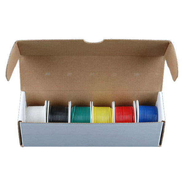 Hook-Up Wire10 metre
Необхідні інструменти ({count})
 Thermal Laminator Machine
 UV LED Array (365nm)
 Digital Microscope
 Soldering Station
 Stopwatch
 Digital Multimeter (Lab Grade)
3
3
The crossover — where each approach actually wins
The crossover — where each approach actually wins
Завантаження блокнота Jupyter…
Необхідні інструменти ({count})
 Desktop ComputerStopwatch
4
4
Compendium — reading the two patents against each other
Compendium — reading the two patents against each other
WHAT DID EACH PATENT ACTUALLY CLAIM? Kilby's, filed February 1959, claims a body of semiconductor material with regions forming the several circuit components and electrical connections between them — and his drawings show gold wires. Noyce's, filed July 1959, claims a structure in which an insulating oxide layer covers the junctions and conductive material is DEPOSITED ON that layer to interconnect the regions. The distinction the courts eventually settled on is exactly the one this pair of blueprints is built around: the components, versus the interconnect.
WHY DID FAIRCHILD LOSE THE PRIORITY FIGHT AND STILL WIN? The Court of Customs and Patent Appeals found for Noyce on the interconnect claims in 1970, but by then it hardly mattered commercially. The companies had cross-licensed in 1966 and everyone building integrated circuits paid both. What decided the industry was not the patent but the manufacturability: Noyce's structure could be made by a process Fairchild already ran, and Kilby's could not be made in volume by anyone.
WHY IS SILICON ESSENTIAL TO NOYCE'S VERSION AND NOT KILBY'S? Because Noyce's depends completely on the oxide, and only silicon has a good one. Kilby's germanium bar needed no oxide — the wires were bonded directly. So the sibling relationship has a materials constraint attached: the hybrid approach is material-agnostic and can integrate gallium arsenide, silicon carbide and silicon in one module, which is a genuine advantage and one reason it persists for radio-frequency and power work.
WHAT WAS THE FIRST COMMERCIAL PRODUCT? Fairchild's Micrologic family from 1961, starting with a flip-flop of four transistors and five resistors. Four transistors. The yield arithmetic from the planar blueprint explains why: at the defect densities of 1961, anything larger yielded nothing.
WHAT DOES THE COMPARISON TEACH THAT NEITHER BLUEPRINT TEACHES ALONE? That an invention can be complete, demonstrated, patented and correct, and still be the wrong answer for the next thirty years because its labour scales with the thing you were trying to eliminate. And that the same invention can be the right answer again later when the surrounding costs change. Kilby's approach did not fail; it waited. Anyone who files these two under duplicate loses precisely that, and it is the most useful thing in either of them.
Матеріали
7- 1 штукаЗаповнювач
- 4 штукЗаповнювач
- 10 штукЗаповнювач
- 1 літрЗаповнювач
- 250 gramЗаповнювач
- 2 штукЗаповнювач
- Hook-Up Wire - Assortment (Stranded)10% комісія10 metre$16.88
Необхідні інструменти
7- Заповнювач
- Заповнювач
- Заповнювач
- Заповнювач
- Заповнювач
- Заповнювач
Орієнтовна сума
Те, що купив майстер. Матеріали без ціни ви купуєте там, де знайдете.
Пов'язані креслення
Ці креслення діляться знаннями — техніки, матеріали або принципи

CC0 Суспільне надбання
Це креслення випущено під ліцензією CC0. Ви можете вільно копіювати, змінювати, поширювати та використовувати цю роботу для будь-яких цілей без запиту дозволу.
Підтримайте мейкера, купуючи продукти через його креслення, де він отримує Комісію мейкера встановлену вендорами, або створіть нову ітерацію цього креслення та включіть його як зв'язок у власне креслення для розподілу доходу.