ART
BEAUTY & WELLNESS
CRAFT
CULTURE & HISTORY
ENTERTAINMENT
ENVIRONMENT
FOOD & DRINKS
REVERSE ENGINEERING
SCIENCES
SPORTS
TECHNOLOGY
WEARABLES
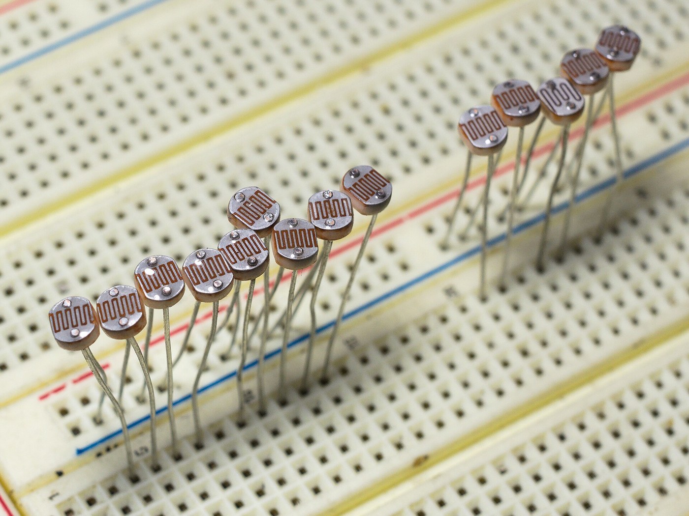


The Selenium Photoconductive Cell
In 1873 Willoughby Smith was not looking for this. He was testing high-resistance materials for the submarine telegraph cable at the Atlantic Telegraph Company, and selenium bars looked promising because their resistance was enormous and stable. Except that it was not stable. His assistant Joseph May noticed the readings wandered, and wandered in a way that tracked the weather: the bars conducted better on bright days and worse when he shut them in a box.
Smith published it in Nature that year under a title that says exactly what happened — the effect of light on selenium during the passage of an electric current. It is the first observation that light can change the electrical properties of a solid, and every electronic image sensor since descends from it.
This blueprint is about the mechanism and about one distinction that is easy to blur and matters enormously.
A PHOTOCONDUCTOR changes its resistance. It generates nothing on its own; you must supply a bias, and what light does is give you more carriers to push. A PHOTOVOLTAIC cell — the silicon solar cell this blueprint links back to — generates its own voltage and needs no bias at all. Same input, entirely different device.
The consequence is the surprising part. A photovoltaic cell can never deliver more than one electron per absorbed photon; that is what quantum efficiency means and it is capped at one. A photoconductor is not capped. If a carrier can cross the gap between the contacts faster than it recombines, it goes round again, and again, and a single photon can be worth hundreds of electrons in the external circuit. Photoconductors have GAIN. That is why they were the sensitive detectors of the early twentieth century and why Baird's television and every light meter used them.
You will measure a real photoconductor across four decades of illumination, extract the power law that describes it, and then find the two ugly properties — the slow response and the memory of what it saw an hour ago — that eventually cost photoconductors the job.
Intermediate
5 hours
Instructions
1
1
What Smith actually found, and why it is not a solar cell
What Smith actually found, and why it is not a solar cell
Selenium in its grey, trigonal, semiconducting form has a bandgap of about 1.8 electronvolts. A photon carrying more energy than that can lift an electron out of the valence band and leave a hole behind, and both are then free to move. 1.8 eV corresponds to a wavelength of about 690 nm, so selenium responds across the whole visible range and stops in the near infrared. That is the entire mechanism, and it took until the 1930s to state it that way, because in 1873 nobody had a band theory to state it with.
HOLD TWO DEVICES APART IN YOUR HEAD.
A photoconductive cell is a bar or a serpentine track of semiconductor with a contact at each end. It is symmetric. It has no junction. In the dark it has a high resistance, and in the light a low one. Put it in series with a resistor and a battery and you have a light-controlled potential divider. That is what Smith had.
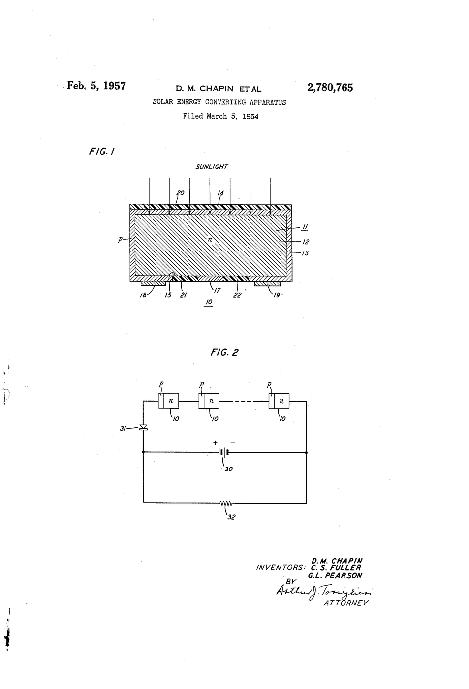
A photovoltaic cell has a junction — in the silicon solar cell blueprint, a p-n junction; in Charles Fritts's 1883 selenium cell, a Schottky barrier between the selenium and a film of gold so thin it was transparent. The junction has a built-in field, so the electron and the hole get swept in opposite directions and a voltage appears across the terminals with no battery anywhere. Fritts's cell was about one percent efficient and he genuinely believed it would compete with coal.
Both were made of selenium. They are not the same invention, and the difference is the junction.
WHY PHOTOCONDUCTORS HAVE GAIN. This is worth being precise about, because it sounds like something for nothing and it is not. A photon makes one electron-hole pair. The applied field sweeps the electron out at the positive contact — but the material must stay neutral, so another electron enters at the negative contact immediately. If the hole is still trapped somewhere in the bulk, that replacement electron also crosses and leaves, and another follows, and this continues until the hole finally finds an electron and recombines.
So the gain is a ratio of two times: how long the slow carrier survives, divided by how long the fast carrier takes to cross. Gain equals carrier lifetime divided by transit time. In cadmium sulfide the lifetime can be milliseconds and the transit time microseconds, so gains of a thousand are ordinary.
And there is the catch that ends the story. The same long lifetime that gives you the gain is what makes the cell slow, because the current cannot stop until those trapped carriers have cleared. Gain and speed are the same number traded in opposite directions. You cannot have both, and television needed both.
A NOTE ON WHAT YOU WILL ACTUALLY USE. Grey selenium cells are now collector items. The standard modern photoconductor is cadmium sulfide, sold everywhere as an LDR or light-dependent resistor, and its physics is identical — a wider gap at 2.4 eV, which is why it peaks in the green at around 540 nm and happens to match the human eye closely enough that light meters used it for fifty years. Everything you measure here is what Smith measured, on a better-behaved material.
Cadmium sulfide is a cadmium compound and is restricted under RoHS, which is why LDRs have become harder to buy. The cell itself is a sealed, coated ceramic disc and is safe to handle. Do not crush, grind or heat it, and do not use one with a cracked coating.
Materials for this step:
 CdS Photoresistor Assortment1 set
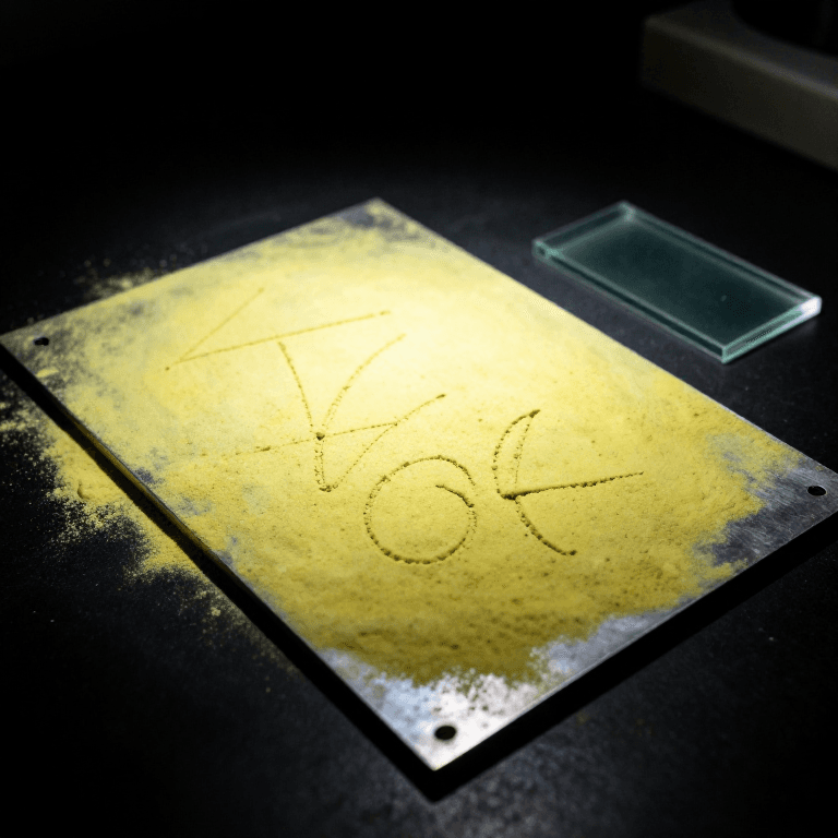
 Selenium Powder5 g
Tools needed:
 Digital Multimeter (Lab Grade)
2
2
Measure the cell across four decades of light
Measure the cell across four decades of light
Photoconductors do not follow a straight line. Resistance falls as illuminance rises, but as a POWER LAW, and the exponent is a property of the material and its trap distribution rather than a universal constant.
Write it as R = A x E^(-gamma), where E is illuminance in lux, A is the resistance at one lux, and gamma is between about 0.5 and 1.0 for cadmium sulfide. A gamma of 1.0 would mean carriers recombine directly with each other; a gamma of 0.5 means recombination is dominated by traps. Real cells sit in between and are not perfectly straight even on log axes.
This sketch does the measurement properly rather than by eye. The LDR sits in a potential divider with a known fixed resistor; the ESP32 reads the midpoint and computes the cell's resistance. A white LED on a PWM output provides the light, and because you are going to sweep it over a wide range, the sketch steps the PWM in a geometric series rather than a linear one — otherwise nine of your ten points land in the bright end and you learn nothing about the dark end.
THE CALIBRATION PROBLEM, STATED HONESTLY. PWM duty cycle is not illuminance. LED output is close to linear in average current, so duty is a decent proxy for RELATIVE illuminance, and that is enough to extract gamma, because gamma comes from the SLOPE of a log-log fit and a constant scale factor only shifts the intercept. If you want A in real ohms-at-one-lux you need a lux meter, and the sketch prints a column for it so you can enter real readings if you have one.
Run the sweep twice: once going up in brightness and once coming down. The two curves will not lie on top of each other. That gap is the next step.
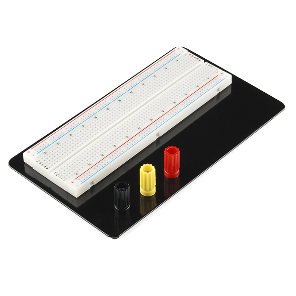
WIRING. LDR from 3V3 to the junction; a 10k fixed resistor from the junction to ground; junction to GPIO34, which is an ADC1 input and safe to use while WiFi is active. The white LED goes from GPIO25 through a 220 ohm resistor to ground. Point the LED at the LDR from about 50 mm with everything inside a closed box, because room light will otherwise dominate your dark readings entirely.
photocell.inocpp
Materials for this step:
CdS Photoresistor Assortment1 set Resistor Kit1 kit
 LED Light Source1 piece
Tools needed:
 ESP32 Development Board
 Breadboard
 Jumper Wire Set
 Lux Meter
 Desktop Computer
3
3
Fit gamma, and compute the gain
Fit gamma, and compute the gain
Loading Jupyter Notebook...
Tools needed:
Desktop Computer4
4
Light history: the cell remembers where it has been
Light history: the cell remembers where it has been
Take the cell you swept in step 2 and do something deliberately unfair to it.
PUT IT IN THE DARK for a full hour with the box closed. Then open the box to a fixed moderate light and start the stopwatch. Read the resistance at 1 s, 5 s, 10 s, 30 s, 60 s, 300 s. It keeps falling. It has not settled after five minutes and in a good cell it will still be creeping after an hour.
NOW REVERSE IT. Leave the cell under a bright lamp for an hour. Then drop it to the SAME moderate light you used before and read the same time series. The resistance climbs, and it approaches the same final value from the other side — but it is not the same value at ten seconds, or at a minute, and depending on the cell it may still be several tens of percent out.
The cell's resistance at any moment is not a function of the light on it now. It is a function of the light on it now AND what it has seen for the last hour. Manufacturers call this light history effect or photoconductive memory, and they specify it as a percentage recovery after a defined dark storage, because there is no way to design it away.
WHY IT HAPPENS is the same traps that gave you the gain. Deep traps fill slowly under illumination and empty slowly in the dark. A cell that has been sitting in the light has a full complement of filled traps, so newly generated carriers have nowhere to fall and stay free longer, so the resistance reads lower than it should. The population takes as long to relax as the traps are deep.
WHAT THIS COST. It is the reason a photographic light meter had to be pointed and then WAITED ON, and the reason serious photographers learned to keep the meter's cell shaded between readings. It is a good part of why the vidicon smeared. And it is why every one of these devices was eventually replaced by junction devices — the photodiode, the CCD, the CMOS pixel — which have no gain, need real amplifiers behind them, and in exchange give you a number that depends only on the photons that arrived during the exposure.
That is the trade the rest of this batch spends its time on: photoconductors, which are sensitive and slow and remember; and junctions, which are fast and honest and need help.
Materials for this step:
CdS Photoresistor Assortment1 setTools needed:
Digital Multimeter (Lab Grade) Stopwatch
Materials
4- Placeholder
- Placeholder
- Placeholder
- Placeholder
Related Blueprints
These blueprints share knowledge with this one — techniques, materials, or principles that connect them in the learning graph.


CC0 Public Domain
This blueprint is released under CC0. You are free to copy, modify, distribute, and use this work for any purpose, without asking permission.
Support the Maker by purchasing products through their Blueprint where they earn a Maker Commission set by Vendors, or create a new iteration of this Blueprint and include it as a connection in your own Blueprint to share revenue.