NGHỆ THUẬT
LÀM ĐẸP VÀ SỨC KHỎE
THỦ CÔNG
VĂN HÓA VÀ LỊCH SỬ
GIẢI TRÍ
MÔI TRƯỜNG
THỰC PHẨM VÀ ĐỒ UỐNG
KỸ THUẬT NGƯỢC
KHOA HỌC
THỂ THAO
CÔNG NGHỆ
THIẾT BỊ ĐEO


The MOSFET
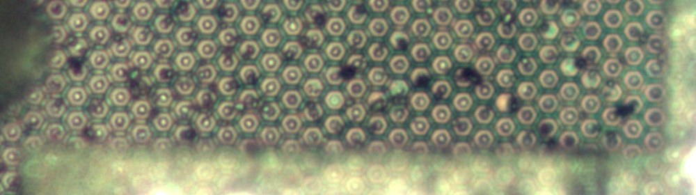
The field-effect transistor is older than the one that made the industry. Julius Lilienfeld patented the idea in 1926: put a voltage on a plate near a semiconductor, and the field should attract carriers into the surface and make it conduct. No current flows into the plate, so control costs nothing. It is a more elegant device than the bipolar transistor in every respect.
It did not work for thirty years, and the reason is one of the great diagnostic stories in physics. Bardeen worked it out in 1947: the surface of a semiconductor is covered in states that trap charge, and the trapped charge screens the field so effectively that almost none of it reaches inside. You can apply the voltage; the surface simply absorbs it. Bardeen and Brattain were investigating exactly that failure when they found the point-contact transistor instead — the bipolar transistor is a consolation prize from a failed FET experiment.
What was needed was a surface with almost no traps, and by 1959 one existed: the thermally grown silicon dioxide interface from Hoerni's planar process, which satisfies all but about one dangling bond in a hundred thousand. Martin Atalla had been studying that passivation directly. He and Dawon Kahng built the metal-oxide-semiconductor field-effect transistor at Bell Labs and demonstrated it in 1960.
It was received without enthusiasm. It was slower than the bipolar transistors of the day, and its threshold voltage drifted because sodium ions in the oxide moved under the gate field. Bell Labs did not pursue it hard.
What it had, and what took a decade to matter, was this: the gate is a capacitor plate, so it draws no steady current at all. A bipolar transistor's base must be fed continuously. Put ten thousand bipolar transistors on a chip and the base currents alone will melt it; put ten thousand MOSFETs on a chip and the static power is nearly zero. Every processor in the world is MOS for that one reason, and the elegance Lilienfeld saw in 1926 turned out to be the property that scaled.
You will measure a real MOSFET, extract its threshold voltage properly, and see the no-gate-current property directly.
Nâng cao
6 hours
Hướng dẫn
1
1
Inversion — how a voltage makes a channel out of nothing
Inversion — how a voltage makes a channel out of nothing
A MOSFET looks impossible at first inspection, and understanding why it is not is the whole physics of the device.
An n-channel MOSFET is built on P-TYPE silicon, whose mobile carriers are holes. Into it are diffused two heavily doped N-TYPE regions, the source and the drain. Between them is p-type silicon, and above that a thin oxide with a metal gate on top.
With no gate voltage, look at the path from source to drain: n-type, then p-type, then n-type. That is two junctions back to back, one of which is reverse-biased whichever way you apply a voltage. No current flows. The device is off, and it is off very well.
Now put a positive voltage on the gate. The gate, oxide and silicon form a capacitor, so positive charge on the gate must be balanced by negative charge in the silicon. At first that happens by pushing the mobile holes away from the surface, leaving behind the fixed negative charge of the acceptor atoms — depletion. Raise the gate voltage further and the depletion region cannot supply any more negative charge, because the acceptors are fixed in place and there are only so many.
So the silicon does something else. It pulls ELECTRONS to the surface — minority carriers, thermally generated and supplied readily by the two n-type regions sitting right there. At a certain gate voltage the electron concentration at the surface exceeds the hole concentration, and a thin sheet of the p-type silicon has become effectively n-type. It has INVERTED.
That inversion layer is a continuous n-type path from source to drain, and current flows. The gate voltage at which it forms is the THRESHOLD VOLTAGE, and it is the single most important parameter of the device.
Three consequences worth holding onto.
The channel is not built, it is INDUCED. Remove the gate voltage and it vanishes. Nothing was doped, nothing was etched; the conducting path is a population of electrons held at the surface by an electric field.
The gate draws no steady current, because there is an insulator under it. It draws a transient current while the capacitance charges, and that is all. This is the property that lets you put billions of them on a chip.
And the source and drain are physically identical. Which one is which is decided by the voltages you apply, not by the construction — the device is symmetric, and in some circuits current genuinely flows both ways.
2
2
Build a curve tracer and measure a real MOSFET
Build a curve tracer and measure a real MOSFET
Datasheets state a threshold voltage. Measuring your own is more instructive, because the number turns out to depend on how you define it and the spread between nominally identical parts is large.
THE CIRCUIT. Source to ground through a 1 ohm sense resistor. Drain to 5 volts through nothing but the ammeter path — the sense resistor does the current measurement. Gate driven by an MCP4725 12-bit DAC, giving about 0.8 millivolt steps over the 0 to 3.3 volt range, which is fine resolution across a threshold that will land somewhere between 1 and 3 volts.
Use a logic-level N-channel part — a 2N7000 for small currents or an IRLZ44N if you want to see real drive capability. Keep the drain current below about 200 milliamps; the sketch stops the sweep there.
WHY A SENSE RESISTOR RATHER THAN A MULTIMETER IN SERIES. Because you want hundreds of readings swept automatically, and because a 1 ohm shunt read by the ADC gives you current and voltage simultaneously at the same instant. The cost is that the shunt drops a little voltage, so the sketch subtracts it to get the true drain-source voltage.
RUN THE TRANSFER SWEEP. The sketch steps the gate from 0 to 3.3 volts and logs gate voltage, drain current and drain-source voltage as CSV. Watch the output: nothing, nothing, nothing, and then current appears and climbs steeply. That knee is the threshold.
THEN DO THE THING THAT PROVES IT IS A FIELD-EFFECT DEVICE. Put your multimeter in series with the gate lead, on its most sensitive current range, and sweep again. The reading stays at essentially zero — picoamps to nanoamps, which is leakage through the oxide and through the meter itself — across the entire sweep, while the drain carries a hundred milliamps.
That is the measurement. A bipolar transistor passing 100 milliamps at a gain of 100 needs a milliamp of base current, continuously, forever. The MOSFET needs none. Multiply by a billion devices and that is why every processor is MOS.
MEASURE THE SPREAD. Sweep five nominally identical parts from the same bag and compare their thresholds. Expect several hundred millivolts of variation. Threshold depends on oxide thickness, substrate doping, work function difference and fixed charge in the oxide, and all four vary across a wafer. That spread is a first-order design constraint, and it is why analogue MOS design leans so heavily on matched pairs made side by side rather than on absolute values.
curve_tracer.inocpp
Vật liệu cho bước này:
 Bo mạch phát triển ESP321 cái
 Mô-đun DAC 12 bit MCP47251 cái
 MOSFET kênh N (2N7000)10 cái
 MOSFET kênh N IRF540N5 cái
 Bộ điện trở chính xác1 bộ
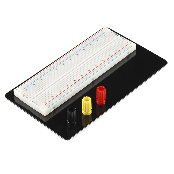 Breadboard1 cái
 Bộ dây nối1 bộ
Công cụ cần thiết:
 Đồng hồ vạn năng số cấp phòng thí nghiệm
 Trạm hàn thiếc
 Nguồn điện để bàn
 Máy hiện sóng
 Máy tính để bàn
3
3
Extract the threshold properly, and see why the gate is a capacitor
Extract the threshold properly, and see why the gate is a capacitor
Đang tải sổ tay Jupyter…
Công cụ cần thiết:
Máy tính để bàn4
4
Compendium — thirty years of not working, then everything
Compendium — thirty years of not working, then everything
WHY DID LILIENFELD'S 1926 PATENT NOT WORK? Surface states. He had the physics right and no way to make a surface clean enough. Bardeen's 1947 surface-state theory explained the failure quantitatively: trapped charge at the semiconductor surface screens the applied field so thoroughly that almost none penetrates. Attempting to verify that theory is what led Bardeen and Brattain to the point-contact transistor — the bipolar transistor exists because the field-effect transistor did not.
WHY DID THE THRESHOLD DRIFT IN EARLY DEVICES? Sodium. Sodium ions are small, positively charged and mobile in silicon dioxide at modest temperatures, so they drift under the gate field and pile up at whichever interface the field pushes them to. Positive charge near the silicon shifts the threshold, so a device biased on for hours came back with a different threshold. It was traced to contamination from handling and glassware, and defeated by obsessive cleanliness plus phosphosilicate glass layers that trap the sodium before it arrives. Almost the entire discipline of semiconductor cleanroom practice descends from chasing this one ion.
WHAT WAS THE SILICON GATE, AND WHY DID IT MATTER SO MUCH? Original MOSFETs used an aluminium gate, deposited AFTER the source and drain were diffused — so the gate had to be aligned to them, and alignment error meant you had to make the gate deliberately oversized to guarantee overlap. That overlap is capacitance between gate and source or drain, and it slows the device badly.
The silicon-gate process, developed by Federico Faggin and Tom Klein at Fairchild around 1968 building on work by Chih-Tang Sah, replaces the metal with heavily doped polycrystalline silicon and deposits it BEFORE the source and drain. The gate then acts as its own mask: the dopant enters everywhere except where the gate shadows it, so the source and drain define themselves against the gate edge with zero alignment error. That is SELF-ALIGNMENT, it removes the overlap capacitance almost entirely, and it is the single change that made MOS fast enough to build a processor from. Faggin took it to Intel and used it to design the 4004.
WHY IS CMOS THE ONE THAT SURVIVED? A single MOSFET switching a resistive load burns power whenever it is on. CMOS pairs an n-channel and a p-channel device so that in either stable state exactly one of them is off — so the path from supply to ground is always broken and static current is essentially zero. Frank Wanlass patented it at Fairchild in 1963. It was ignored for years because it needs both device types and therefore more process steps and more area. It won when power density, not area, became the binding constraint, which happened in the 1980s and has never stopped being true.
WHY DID THE GATE OXIDE STOP SHRINKING? It reached about 1.2 nanometres, five atomic layers, and electrons began tunnelling straight through it. Leakage through the gate started to rival the switching power. The fix was to stop using silicon's own oxide for the gate and adopt hafnium-based high-permittivity dielectrics around 2007, which give the same capacitance from a physically thicker film. Fifty years of running on the material's own oxide ended there, for a quantum-mechanical reason.
WHAT IS THE HONEST SUMMARY? The MOSFET was invented first, worked last, was unimpressive when it finally worked, and then turned out to have the one property — no static control current — that mattered more than everything the bipolar transistor was better at. That is a reasonably common shape for a technology, and it is worth remembering the next time something is dismissed for being slower.
Vật liệu
7- Tạm thời
- Tạm thời
- 10 cáiTạm thời
- Tạm thời
- Tạm thời
- Breadboard - ClassicHoa hồng 10%1 cái$9.40
- 1 bộTạm thời
Công cụ yêu cầu
5- Tạm thời
- Tạm thời
- Tạm thời
- Tạm thời
Tổng ước tính
Những gì người làm đã mua. Vật liệu không hiện giá thì bạn mua ở đâu tuỳ bạn.
Blueprint liên quan
Các blueprint này chia sẻ kiến thức — kỹ thuật, vật liệu hoặc nguyên tắc


CC0 Phạm vi công cộng
Bản thiết kế này được phát hành theo CC0. Bạn tự do sao chép, sửa đổi, phân phối và sử dụng cho bất kỳ mục đích nào mà không cần xin phép.
Hỗ trợ nhà sáng tạo bằng cách mua sản phẩm qua bản thiết kế, nơi họ nhận Hoa hồng nhà sáng tạo do nhà bán hàng đặt, hoặc tạo phiên bản mới và kết nối trong bản thiết kế riêng để chia sẻ doanh thu.