UBUCIKO
UBUHLE NEMPILO
UBUCIKO BEZANDLA
AMASIKO NOMLANDO
EZOKUZIJABULISA
IMVELO
UKUDLA NEZIPHUZO
REVERSE ENGINEERING
IZAYENSI
EZEMIDLALO
UBUCHWEPHESHE
IZINTO EZIGQOKWAYO
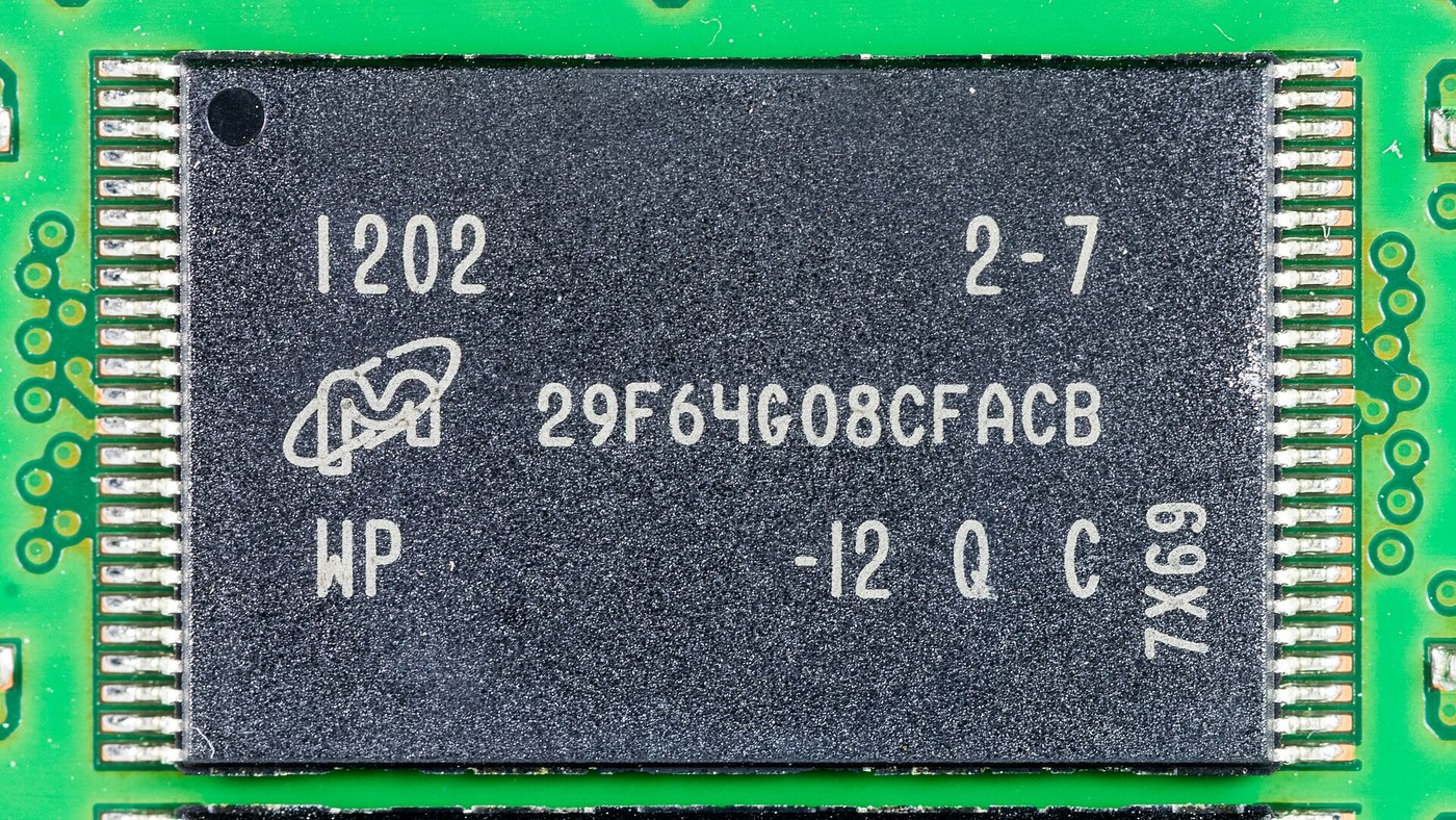


Flash Memory
This is the sibling of `eprom-floating-gate`. Same storage mechanism — electrons trapped on an island inside the gate oxide — and a completely different way of getting them off again, which changes what the device is for.
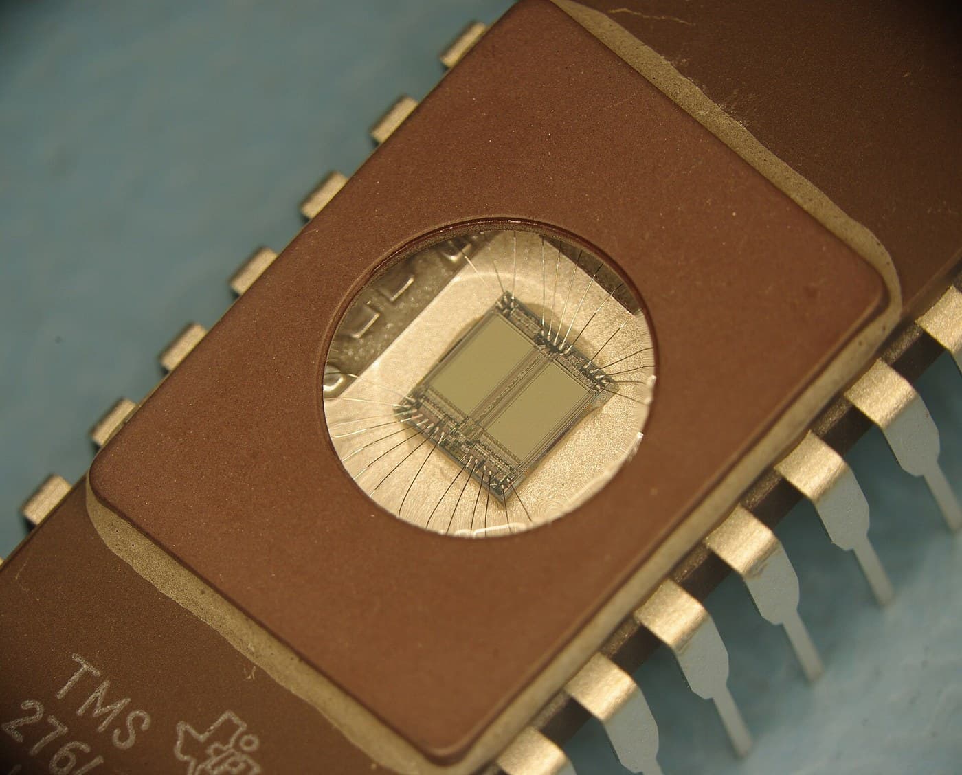
An EPROM is erased by ultraviolet light through a quartz window. That means the part must be physically removed from the board, put under a lamp for twenty to thirty minutes, and returned. The whole chip erases together; there is no such thing as erasing part of it. The quartz window is also expensive, which is why one-time-programmable EPROMs in cheap plastic packages existed in parallel: the identical die, without the window, erasable never.
Fujio Masuoka at Toshiba proposed the change in 1980 and presented it in 1984: erase ELECTRICALLY, in place, by tunnelling the electrons back off the floating gate through a thinner oxide under a strong field. No lamp, no window, no removal from the board.
But not one bit at a time. The erase field has to be applied to a whole region at once, so flash erases in BLOCKS — tens of kilobytes at a time in early parts, megabytes in modern ones. You can program individual bytes or pages, and you can only erase in large chunks, and you can only program a bit from 1 to 0. To turn a 0 back into a 1 you must erase its entire block.
That single asymmetry is where every strange thing about flash comes from. It is why a flash device needs a controller doing wear levelling and garbage collection rather than presenting itself as plain memory. It is why writing 4 kilobytes can cause megabytes of internal activity. And it is why solid-state drives have a firmware layer more complicated than some operating systems.
The name, incidentally, came from a colleague of Masuoka's who said the block erase reminded him of a camera flash.
You will measure endurance on real parts by wearing one out deliberately, and watch the erase-block behaviour that the whole architecture is built around.
Ophakathi
5 hours
Imiyalelo
1
1
Prove the asymmetry — program a byte, then try to un-program it
Prove the asymmetry — program a byte, then try to un-program it
One experiment establishes the entire character of the device, and it takes ten minutes.
USE A SERIAL NOR FLASH — a W25Q32 or similar, on a breakout board, driven over SPI from an ESP32 or an Arduino. These cost very little, the command set is simple and documented, and unlike an SD card there is no controller hiding what is happening.
STEP ONE. Erase a sector — command 0x20, sector erase, 4 kilobytes. Read it back. Every byte is 0xFF. Erased means all ones.
STEP TWO. Program one byte to 0x0F using the page program command. Read it back: 0x0F. Fine.
STEP THREE, and this is the one that matters. Program that SAME byte to 0xF0. Read it back.
You will not get 0xF0. You will get 0x00.
Think about what happened. Programming can only pull bits DOWN, from 1 to 0 — it adds electrons to floating gates, and there is no per-bit way to take them off. The device did a bitwise AND of what was there with what you asked for: 0x0F AND 0xF0 is 0x00. It did not refuse, it did not report an error, it did exactly what the hardware can do and returned success.
STEP FOUR. Erase the sector again and program 0xF0. Now it works, because the erase restored every bit to 1 first.
That is flash, completely. Programming clears bits; erasing sets them, and only in blocks. Everything else in a solid-state drive is software built to hide this.
NOW SEE THE BLOCK GRANULARITY. Write a recognisable pattern across a whole 4 kilobyte sector. Then erase and observe that you cannot erase less: there is no command to erase 100 bytes. Try modifying one byte in the middle of the sector from 0 back to 1, and find that the only route is to read the entire sector into RAM, erase it, modify the copy, and write all 4 kilobytes back.
TIME THAT SEQUENCE and compare it with the time to program 4 kilobytes into an already-erased sector. The read-modify-erase-write cycle is far slower, and it wrote 4096 bytes to change one. That ratio is WRITE AMPLIFICATION, it is the central problem of flash storage, and you have just measured it on your own bench.
Izinto zokwakha zalesi sinyathelo:
 Imojula yenkumbulo ye-flash ye-SPI W25Q325 izicucu
 Ibhodi Lokuthuthukisa le-ESP321 ucezu
 Ibhodi Lokuhlola1 ucezu
 Izintambo Zokuxhuma1 isethi
Amathuluzi adingekayo:
 Ikhompyutha Yasetafuleni
 I-Multimeter Yedijithali Yezinga Lelabhorethri
 I-Oscilloscope
 Iwashi Lokumisa Isikhathi
2
2
Wear one out on purpose
Wear one out on purpose
Endurance is a specification everyone quotes and almost nobody measures. It is measurable on a bench in a day, and the result is more interesting than the datasheet number.
WRITE A CYCLING LOOP. Pick one sector. Repeatedly: erase it, program the whole sector with a known pattern, read it back, and count any bytes that differ. Log the cycle number and the error count. Leave it running.
Use a sacrificial part and confine the cycling to ONE sector so the rest of the device stays healthy as a control.
WHAT TO EXPECT. A NOR flash rated at 100,000 cycles will typically go tens of thousands of cycles with zero errors, then start producing occasional single-bit failures, then fail more often, and then fail persistently in particular bytes. Plot errors against cycle count.
The curve is not a cliff and it is not linear. It is flat, then a knee, then a steep rise — and crucially the failures cluster: the same few cells fail again and again while their neighbours are fine. That clustering is the whole justification for wear levelling. If failure were uniform there would be nothing to level.
WATCH THE ERASE TIME AS WELL AS THE ERRORS, because it is the better early warning. Time each erase operation. As the oxide accumulates trapped charge from repeated tunnelling, erasing gets harder and the internal state machine takes longer — and this happens well before any bit actually fails. A rising erase time is a worn block announcing itself, and real controllers watch exactly this.
WHY IT WEARS. Every program and erase drives electrons through the tunnel oxide at high field. A fraction do not make it cleanly through and get stuck in the oxide itself. Trapped charge does two things: it screens the field, so subsequent erases need longer, and it eventually forms a conductive path that lets the floating gate leak. The cell stops holding its bit.
The honest framing, which the popular version gets backwards: flash does not wear out from being READ. Reads are gentle. It wears from being ERASED, and the erase count is what a controller tracks.
IF YOU HAVE THE PATIENCE, run a second part at elevated temperature — 60 or 70 degrees — and compare. Wear is thermally accelerated, and hot flash dies sooner. That is why an SSD in a badly ventilated laptop has a genuinely shorter life than the same drive in a cool desktop.
Izinto zokwakha zalesi sinyathelo:
Imojula yenkumbulo ye-flash ye-SPI W25Q325 izicucuIbhodi Lokuthuthukisa le-ESP321 ucezu Inzwa yokushisa i-DS18B201 ucezuIbhodi Lokuhlola1 ucezu
Amathuluzi adingekayo:
Ikhompyutha YasetafuleniIwashi Lokumisa Isikhathi Ithemomitha Yaselabhorethri
 Umthombo Kagesi Wasebhentshini
3
3
Cycle a sector until it dies
Cycle a sector until it dies
Wearing a part out is the only honest way to see the shape of flash failure, and it needs tens of thousands of cycles, which is a loop rather than a person.
This sketch cycles ONE sector — erase, program the whole sector, verify — and logs three things per cycle: the erase time in microseconds, the count of bytes that came back wrong, and the address of the first bad byte.
The third column is the one people forget to record, and it is where the interesting result is. Failures CLUSTER: the same addresses fail again and again while their neighbours stay perfect. If wear were uniform there would be no such thing as wear levelling, and this column is the evidence that it is not.
The erase-time column is the early warning. Trapped charge accumulating in the tunnel oxide screens the erase field, so the internal state machine needs longer — and this rises measurably before any bit actually fails. A real controller retires a block on exactly this signal rather than waiting for data loss.
It verifies after the ERASE as well as after the program, because a worn cell often fails to erase to 0xFF before it fails to hold a programmed 0. Checking only the programmed state misses the first half of the failure.
This destroys a real device. Use a sacrificial part, confine the cycling to one sector so the rest of the chip remains as a control, and expect it to take hours.
flash_wear.inocpp
Amathuluzi adingekayo:
Ikhompyutha YasetafuleniIbhodi Lokuthuthukisa le-ESP32I-Oscilloscope4
4
Tunnelling, endurance and write amplification
Tunnelling, endurance and write amplification
Ilayisha incwadi ye-Jupyter…
Amathuluzi adingekayo:
Ikhompyutha YasetafuleniIzinto
5- Isibambeli
- Isibambeli
- Isibambeli
- Isibambeli
- 1 ucezuIsibambeli
Amathuluzi Adingekayo
7- Isibambeli
- Isibambeli
- Isibambeli
- Isibambeli
- Isibambeli
- Isibambeli
Ama-blueprint ahlobene
Lama-blueprint abelana ngolwazi — amasu, izinto noma izimiso


CC0 Isizinda Somphakathi
Le blueprint ikhishwe ngaphansi kwe-CC0. Ukhululekile ukukopisha, ukuguqula, ukusabalalisa, nokusebenzisa ngaphandle kwemvume.
Sekela uMenzi ngokuthenga imikhiqizo nge-Blueprint yabo IKhomishane Yomenzi kumiswe ngabathengisi, noma dala inguqulo entsha yale Blueprint bese uyifaka njengoxhumaniso ku-Blueprint yakho ukuze wabelane ngemali engenayo.