Etching a Printed Circuit Board at Home — Toner Transfer Method
Instruções
Design and Print the Circuit Layout
Design and Print the Circuit Layout
Design the circuit layout in PCB design software (KiCad, EasyEDA, Eagle, or Fritzing). The layout must be printed as a mirror image because it will be transferred face-down onto the copper. Print the layout on glossy photo paper using a laser printer at the highest toner density setting. Laser printer toner is a plastic polymer that bonds to the copper surface when heated, acting as an etch resist — inkjet ink will not work because it is water-based and dissolves in the etchant. The trace widths should be at least 0.3mm for reliable home etching (professional PCB factories can go much finer). Print a test copy on regular paper first and hold it against the copper-clad board to verify sizing.
Materiais para este passo:
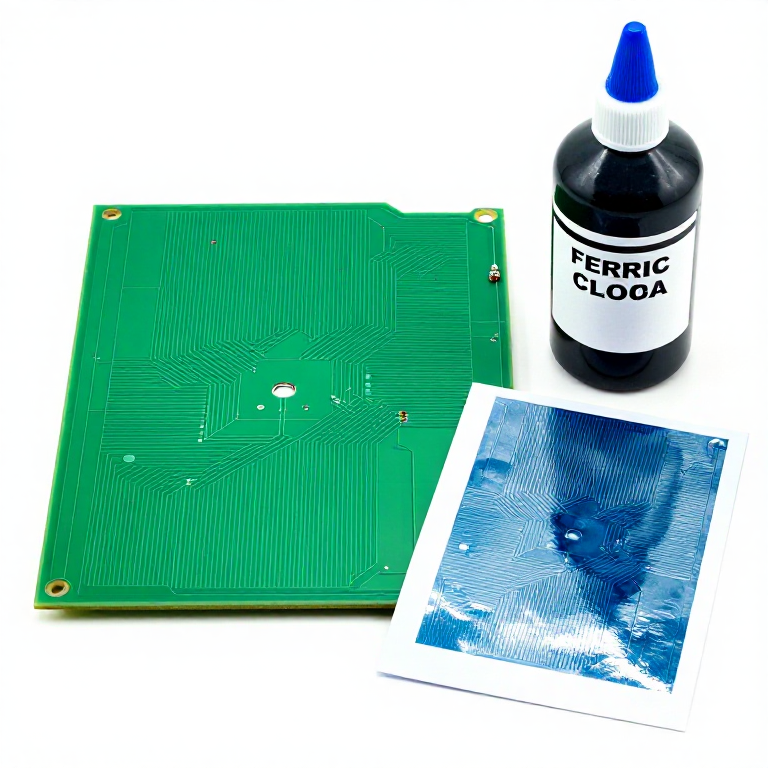
 PCB Blank (Copper Clad)1 piece, sized for your circuit peça
 Acid Etching Solution (Ferric Chloride)200-500ml ml
 Acetone50ml ml
 Steel Wool1 piece peça
Prepare the Copper Surface and Transfer Toner
Prepare the Copper Surface and Transfer Toner
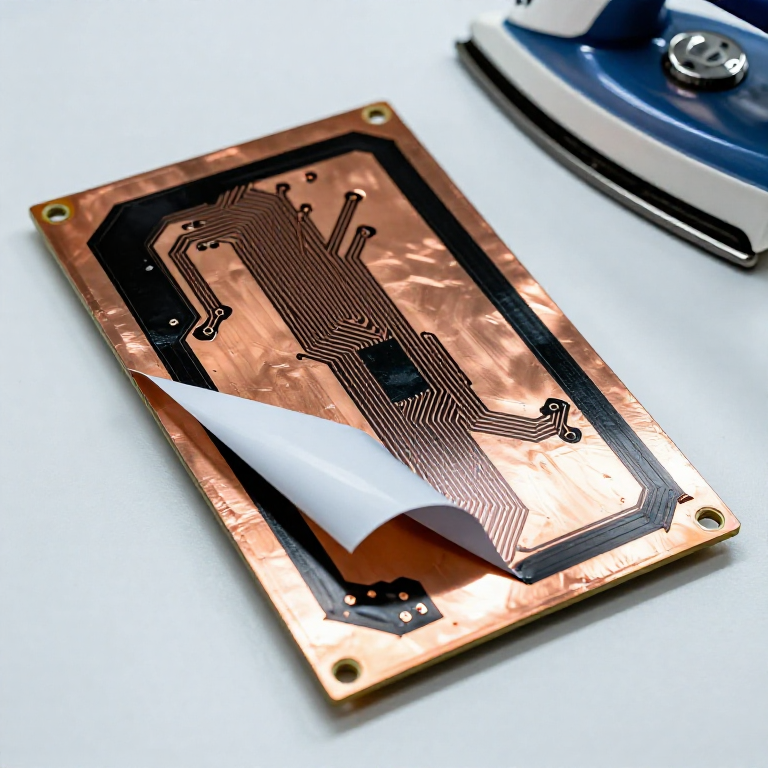
Clean the copper surface of the PCB blank by scrubbing with fine steel wool or a Scotch-Brite pad until it is uniformly bright and shiny with no oxidation, fingerprints, or grease. Any contamination prevents toner adhesion. Handle the cleaned board by the edges only. Place the printed glossy paper face-down on the cleaned copper surface, aligning the circuit layout. Apply heat and pressure with a clothes iron set to the highest heat (no steam). Press firmly and evenly for 3-5 minutes, moving the iron slowly across the entire surface. The heat melts the toner (approximately 180 degrees C), and the pressure bonds it to the copper. Allow to cool slightly, then soak the board in warm water for 10-15 minutes until the paper softens and peels away, leaving the toner pattern on the copper.
Inspect and Touch Up the Transfer
Inspect and Touch Up the Transfer
Inspect the transferred toner pattern carefully under bright light. Look for any areas where the toner did not transfer cleanly — breaks in traces, pinholes, or missing pads. Touch up any defects using a permanent marker (Sharpie) or PCB resist pen — the marker ink acts as etch resist just like the toner. This inspection step is critical: a single break in a trace means a broken electrical connection in the finished board, which can be very difficult to diagnose later. Pay particular attention to fine traces and the spaces between closely spaced pads — these are the most common failure points in toner transfer.
Etch the Board
Etch the Board
Wearing safety gloves and goggles (ferric chloride stains permanently and is mildly corrosive), pour ferric chloride solution into a plastic etching tray to a depth of approximately 1cm. Submerge the board copper-side down, floating it on the surface of the etchant. Gently agitate the tray every minute by rocking it back and forth — agitation brings fresh etchant to the copper surface and speeds the process. Etching takes 15-45 minutes depending on the solution temperature and freshness (warmer etchant works faster, 40-50 degrees C is optimal). Check progress periodically by lifting the board — you will see the copper gradually dissolving from around the toner-protected traces. Etching is complete when all exposed copper has dissolved, leaving only the traces protected by toner. Do not over-etch, as the solution will undercut beneath the toner edges, thinning the traces.
Clean, Drill, and Finish
Clean, Drill, and Finish
Remove the etched board from the solution, rinse thoroughly with water, and remove the toner with acetone or nail polish remover, revealing the bright copper traces beneath. Inspect the traces for continuity — use a multimeter in continuity mode to verify that each trace connects its intended points without short circuits to adjacent traces. Drill component holes using a 0.8-1.0mm drill bit in a small drill press or rotary tool. PCB drill bits are carbide because fibreglass (FR4) is extremely abrasive and dulls steel bits instantly. After drilling, lightly sand the copper with fine steel wool to remove any oxidation and improve solderability. The finished board is ready for component soldering. For longer-term protection, apply a flux coating or clear lacquer to the copper to prevent oxidation before components are installed.
Materiais
5- 1 piece peçaReferência
- Glossy Photo Paper1-2 sheets peça
- 200-500 ml peçaReferência
- 1 piece peçaReferência
Ferramentas necessárias
5- Laser Printer
- Plastic Etching Tray
- Referência
- Referência
Related blueprints
Other builds that share materials, tools, or techniques with this one.
CC0 Domínio Público
Este blueprint é liberado sob CC0. Você é livre para copiar, modificar, distribuir e usar este trabalho para qualquer finalidade, sem pedir permissão.
Apoie o Maker comprando produtos através do Blueprint, onde ele ganha uma Comissão Maker definida pelos vendedores, ou crie uma nova versão deste Blueprint e inclua-o como conexão no seu próprio Blueprint para compartilhar receita.