LIST
FEGURÐ OG VELLÍÐAN
HANDVERK
MENNING OG SAGA
SKEMMTUN
UMHVERFI
MATUR OG DRYKKUR
ÖFUGVERKFRÆÐI
VÍSINDI
ÍÞRÓTTIR
TÆKNI
KLÆÐANLEG TÆKNI


The Chip-on-Board Breakout: From a 0.4 mm Mezzanine to Pins You Can Reach
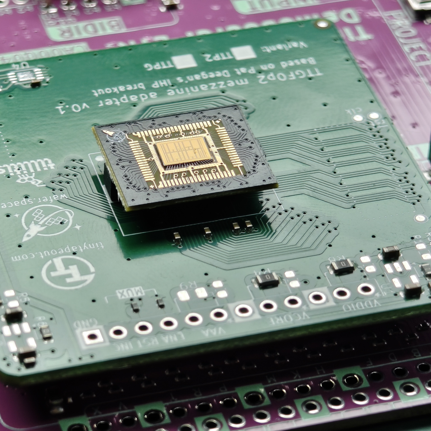
A chip from a shared wafer comes back tiny. On wafer.space's Run 1 it arrived as a chip-on-board part 14 × 16 mm, with the die wire-bonded under epoxy and a 70-pin mezzanine connector underneath at 0.4 mm pitch. Nothing on a bench can touch pins that small, so the first thing to build is a board that carries them back out.
wafer.space publishes example breakout motherboards in KiCad under Apache-2.0: one sheet, two boards. Each has the mating 70-pin mezzanine socket; one breaks the pins out to two 1 × 35 rows of 0.1-inch pin headers, the other to two rows of 35 castellated edge pads at 1 mm.
This rung works out why the fine pitch is needed and what spreading it out costs in board length, shows the published schematic, and builds the header version.
Lengra kominn
About a day of soldering, plus board fabrication
Leiðbeiningar
1
1
Pitch against board edge
Pitch against board edge
Hleð Jupyter-vinnubók…
2
2
Where the chip comes from
Where the chip comes from
The embedded blueprint designs the chip and orders it. This rung builds the board it plugs into.
3
3
What the chip-on-board plugs into
What the chip-on-board plugs into
From wafer.space's Run 1 documentation: the full-slot chip-on-board is 14 × 16 mm; the die's 74 bond pads follow the Tiny Tapeout convention, and all grounds are tied together on the default breakout. It carries a 70-pin, 0.4 mm pitch mezzanine connector (LCSC C19089236; the mating part is LCSC C19089262).
So that every project fits the same boards, the default breakouts share the same wire-bonding layout, the same 14 × 16 mm footprint and the same connector position; traces, signal types and net assignments are left to the designer. wafer.space notes that pinouts, connectors and footprints are specific to each run.
4
4
The published breakout schematic
The published breakout schematic
wafer.space's example motherboards, from the chip-on-board-wire-bonded-pcbs repository (run-1/motherboards, Apache-2.0), shown as published. On the left, the ".1\" Header" board: the mezzanine socket J102 (HCTL HC-PBB40C-70DP-0.4V-02, 70 pins at 0.4 mm) broken out to the 1 × 35 pin headers J101 and J103 at 2.54 mm. On the right, the "Castellated" board: the same socket J105 broken out to the 1 × 35 castellated edges J104 and J106 at 1 mm, so the whole breakout can itself be soldered onto a larger board.
Hleður KiCanvas skoðara...
Faglegur PCB hönnunarskoðari
5
5
Build the header board
Build the header board
Download the run-1/motherboards project from the repository and open it in KiCad. The files are saved by KiCad 10, so an older KiCad will not open them. Plot the Gerber and drill files and order the board from a PCB fabricator, with a solder-paste stencil for the mezzanine footprint.
Hold the stencil over the mezzanine pads and spread lead-free solder paste across it in one stroke. Place the socket with fine tweezers, square to its pads, and reflow it with the hot-air station until the paste flows and settles. Inspect every one of the 70 joints with the loupe; clear any bridge between neighbouring pins with flux and the iron or hot air.
Solder the two 1 × 35 pin headers with the iron. Before you plug in a chip, check with the multimeter that no two neighbouring header pins are shorted, and that each header pin reaches the socket pin the schematic connects it to.
Efni fyrir þetta skref:
 Prentplata1 stykki
 Tengi milli rafrásaborða1 stykki
 Pinnaröð2 stykki
 Lóðmálmsmauk (blýlaust)1 stykki
 Tin-blý lóðmálmur1 stykki
 Lóðfeiti1 stykki
Nauðsynleg verkfæri:
 Heitloftsviðgerðarstöð
 Lóðbolti
 Oddmjóar pinsettur
 Stækkunarlúpa
 Fjölsviðsmælir
 Borðtölva
6
6
A breakout that shorts or does not connect
A breakout that shorts or does not connect
Breakout board troubleshooting.
Flow
Loading...
7
7
Sources and honest limits
Sources and honest limits
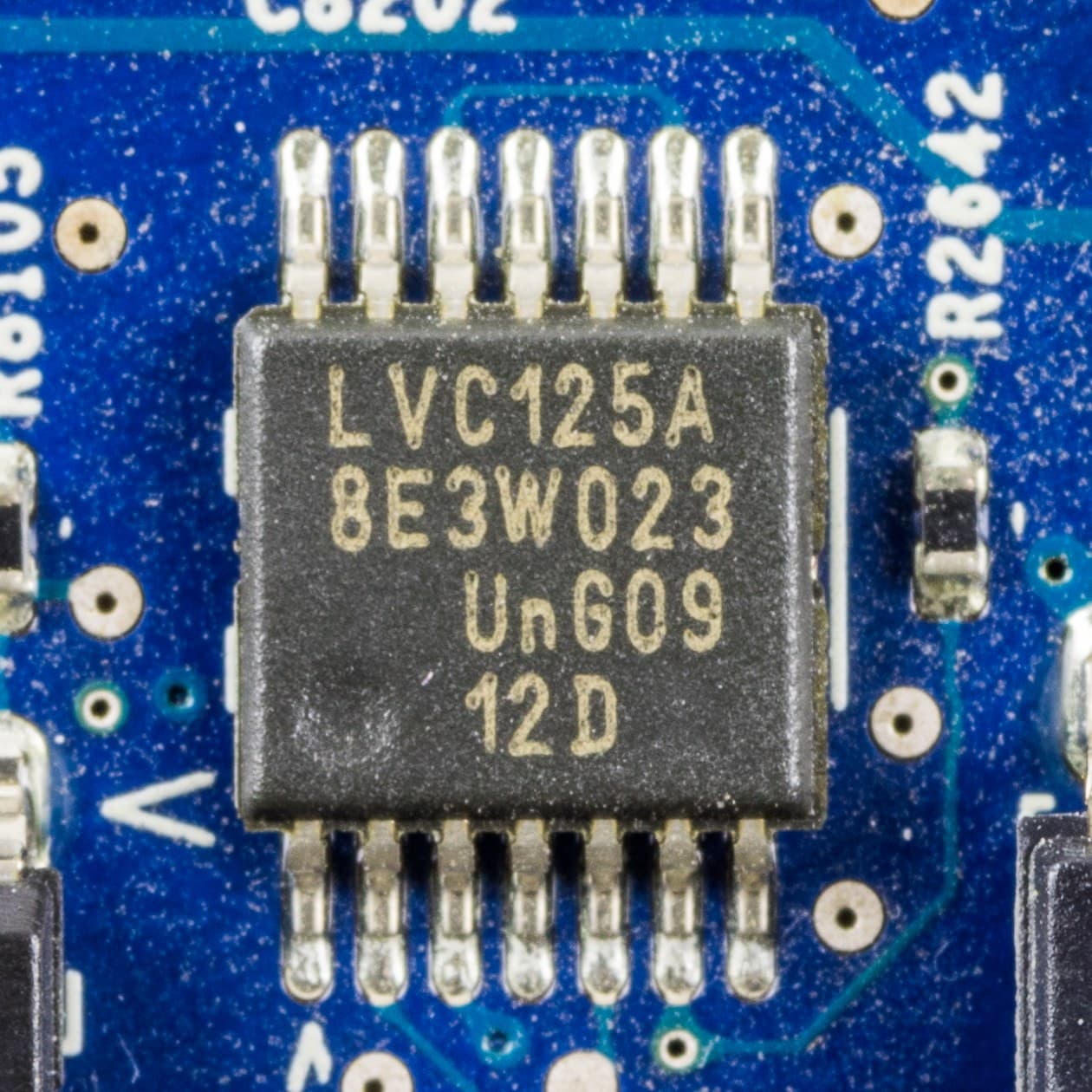
**Sources**, read 29 September 2026: wafer.space's chip-on-board-wire-bonded-pcbs repository (README, run-1/README and run-1/motherboards, Apache-2.0). The schematic in step 4 is theirs, unchanged. The photograph is theirs too, from the same repository: a Run 1 chip-on-board seated on a Tiny Tapeout mezzanine adapter board (TTGF02, v0.1), not the header board built in step 5.
**Honest limits.** This rung has not been built for this blueprint; the soldering steps are standard practice for a 0.4 mm surface-mount connector, not wafer.space instructions. The pinout and footprint are Run 1's, and wafer.space says they are expected to change in later runs, so check the current run's documentation before ordering boards.
Efni
6- 1 stykkiStaðgengill
- 1 stykkiStaðgengill
- 1 stykkiStaðgengill
- 1 stykkiStaðgengill
- 1 stykkiStaðgengill
Nauðsynleg verkfæri
6- Staðgengill
- Staðgengill
- Staðgengill
- Staðgengill
- Staðgengill
Tengd Blueprint
Þessi blueprint deila þekkingu — tækni, efni eða meginreglur


CC0 opinbert ríki
Þessi teikning er gefin út undir CC0. Þér er frjálst að afrita, breyta, dreifa og nota þetta verk í hvaða tilgangi sem er, án þess að biðja um leyfi.
Studdu smiðinn með því að kaupa vörur í gegnum teikningu hans þar sem hann fær þóknun smiða sem seljendur ákvarða, eða búðu til nýja endurskoðun á þessari teikningu og tengdu hana sem tengingu í þinni eigin teikningu til að deila tekjum.