कला
सुन्दरता र कल्याण
हस्तकला
संस्कृति र इतिहास
मनोरञ्जन
वातावरण
खाना र पेय
रिभर्स इन्जिनियरिङ
विज्ञान
खेलकुद
प्रविधि
पहिर्न मिल्ने
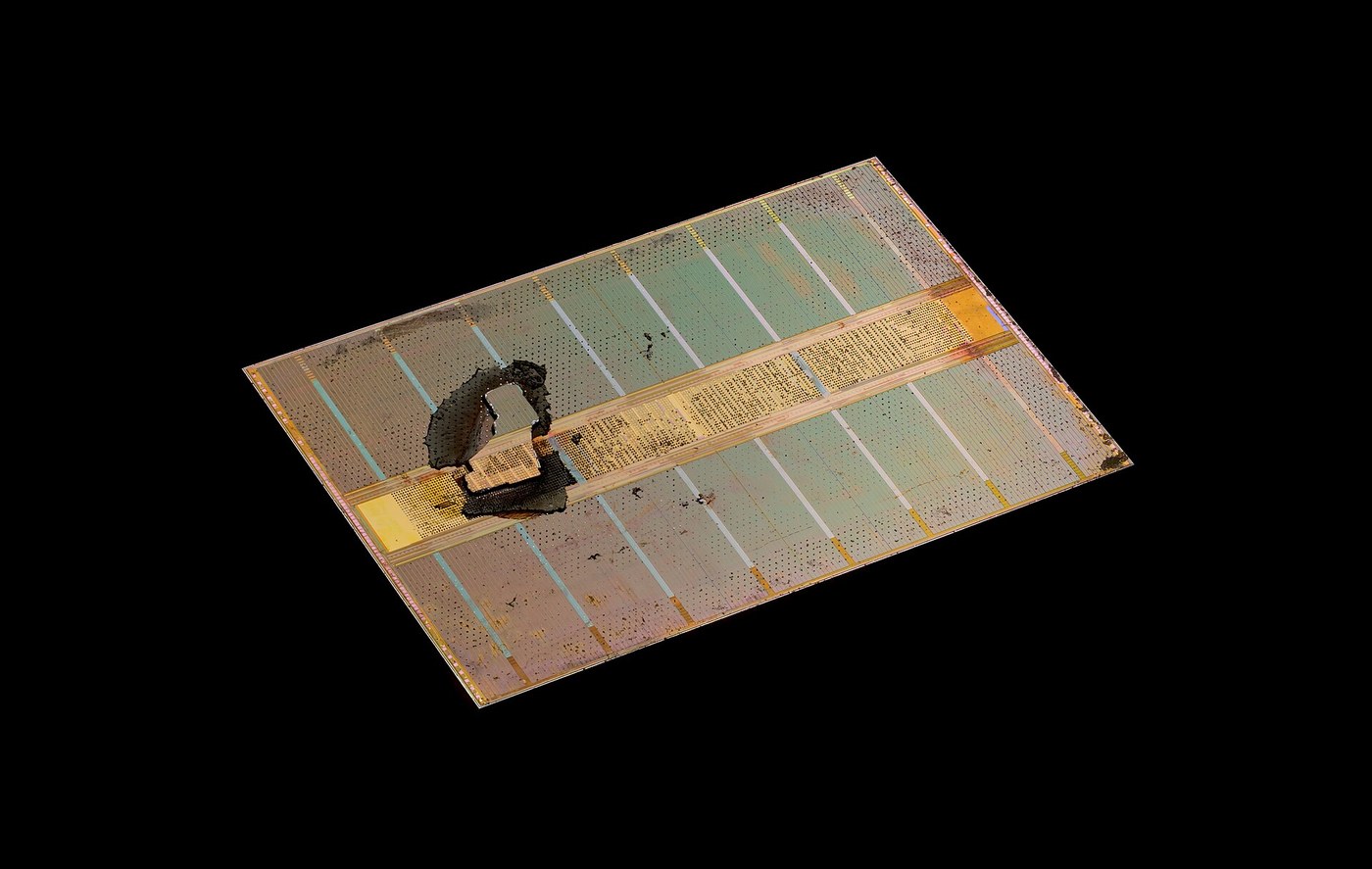


The Sense Amplifier
The DRAM cell holds about 25 femtofarads of charge. The bit line it has to talk to is a wire running past thousands of other cells, and it carries 200 to 400 femtofarads of its own capacitance. When the access transistor opens, those two capacitances share their charge — and the cell, being ten to thirty times smaller, loses the argument almost completely.
The result is that reading a DRAM cell produces a signal of roughly 50 to 100 millivolts on a line that swings a volt or more. The information is there, and it is buried in a fraction of the noise budget of everything around it.
The sense amplifier is what recovers it, and the way it does so is one of the most elegant tricks in circuit design: it is the SAME cross-coupled latch as the SRAM cell in the previous blueprint, wired across the bit line pair, but used as an amplifier rather than as storage.
Both bit lines are pre-charged to exactly half the supply and left floating. The cell tips one of them slightly. Then the latch is powered up — and a latch is a circuit with two stable states and an unstable point exactly between them, so a latch released from the unstable point falls towards whichever stable state the tiniest imbalance favours. The 50 millivolt difference decides which way it falls, and the latch's own positive feedback drives it the rest of the way to a full logic level.
It is a coin balanced on its edge, tipped by a breath, and it lands decisively.
Two consequences follow. Because the latch ends up driving the bit line hard to a full rail, and because the cell is still connected, the amplifier automatically WRITES THE BIT BACK — which is exactly what a destructive read requires, and it is free. And because a latch has no idea what it is amplifying, firing it before the signal has developed makes it decide on noise, confidently and wrongly. The timing of that fire signal is one of the tightest constraints in the whole part.
You will build one from discrete parts, feed it a deliberately tiny difference, and find the smallest signal it can resolve.
उन्नत
5 hours
निर्देशनहरू
1
1
The latch, used as an amplifier
The latch, used as an amplifier
Compare this schematic with the SRAM cell in the previous blueprint. The four transistors in the middle are the same circuit — two inverters, cross-coupled. The difference is entirely in how it is used.
In SRAM the latch is permanently powered and holds a bit. Here its supply rails are SWITCHED: SAP is pulled up and SAN pulled down only at the moment of sensing. Between reads the latch is unpowered and its nodes float at the pre-charge level.
That is the whole trick. An unpowered latch sitting with both nodes at exactly VDD over 2 is at its unstable equilibrium point. It has two stable states either side and it is balanced precisely between them. Apply power and it must fall one way, and which way is decided by any asymmetry present at that instant — including a 50 millivolt difference put there by a memory cell.
NOTE Cbl IN THE SCHEMATIC. That capacitor is not a component anybody fitted; it is the bit line's own parasitic capacitance, drawn because it dominates the problem. It is the wire's capacitance to the substrate and to its neighbours, accumulated over the length of the array, and it is ten to thirty times the cell it is trying to read.
That ratio is the reason DRAM arrays are divided into sub-arrays with their own sense amplifiers. Making the bit line longer puts more cells on it, which is good for density, and adds capacitance, which shrinks the signal. Somewhere around 256 to 512 cells per bit line the signal gets too small to sense reliably, and that number — not the process — sets the sub-array size in every DRAM ever made.
WHY BOTH BIT LINES. The amplifier is differential, and a reference is needed. In the folded bit line arrangement the pair runs side by side, so noise coupling from neighbouring lines lands on BOTH equally and cancels in the difference. The cell only ever tips one of them. That common-mode rejection is why the layout looks the way it does, and it is worth more than any amount of shielding.
KiCanvas दर्शक लोड गर्दै...
व्यावसायिक PCB डिजाइन दर्शक
चाहिने औजार:
 टेबुल कम्प्युटर
2
2
Build one and find the smallest signal it can resolve
Build one and find the smallest signal it can resolve
Build the latch from discrete transistors rather than a logic IC, because you need access to the supply rails to switch them.
THE LATCH. Two 2N7000 n-channel and two BS250 p-channel MOSFETs, or a CD4007 which gives you three complementary pairs in one package and is far easier. Cross-couple two inverters. Bring both supply rails out to switchable pins: SAP to a p-channel switch from VDD, SAN to an n-channel switch to ground.
THE BIT LINES. Two 220 picofarad capacitors, one on each node, standing in for the bit line capacitance. Two more switches to pre-charge both nodes to VDD over 2 from a divider, and an equalising switch shorting the two nodes together — that equaliser matters, because it forces the two sides to start genuinely equal rather than merely nominally equal.
THE SIGNAL. A third capacitor, 10 picofarads, standing in for the cell, charged separately to a level you set, and dumped onto one node through a switch. The ratio of 10 to 220 gives you roughly the same charge-sharing attenuation a real cell suffers.
THE SEQUENCE, and the order is not negotiable:
Equalise and pre-charge both nodes to VDD over 2, then open the pre-charge and equalise switches so both float.
Dump the cell charge onto one node. Measure the difference on the scope — it should be tens of millivolts.
Wait a defined delay.
Fire SAP and SAN together.
Watch the nodes separate to the rails.
FIND THE SENSITIVITY. Reduce the cell voltage step by step and repeat, twenty times at each level, recording how often the amplifier lands on the correct side. Plot the error rate against the input difference.
You will get an S-curve, not a threshold. Well above some level it is always right; well below it is a coin toss; and in between there is a band where it is right most of the time. That band is where offset and noise live, and its width tells you what your latch's own asymmetry is.
NOW FIRE IT EARLY. Reduce the delay between the cell dump and the fire until the amplifier does not have time to see the full signal. The error rate climbs. Keep going and it approaches 50 percent — and notice that it never announces a problem. It produces a confident, full-swing, completely wrong answer. That silent confidence is why sense amplifier timing is designed with margin rather than optimised to the edge.
यस चरणका सामग्री:
 CD4007 CMOS ट्रान्जिस्टर सरणी5 टुक्रा
 N-च्यानल MOSFET (2N7000)10 टुक्रा
 सेरामिक क्यापासिटर किट1 सेट
 प्रतिरोधकको सेट1 सेट
 तार्किक आईसीको विविध सेट1 सेट
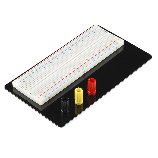 Breadboard2 टुक्रा
चाहिने औजार:
 तरङ्गदर्शी
 बेन्चको विद्युत् आपूर्ति
 प्रयोगशाला स्तरको डिजिटल बहुमापक
 ESP32 विकास बोर्ड
3
3
Sequence it and sweep the sensitivity
Sequence it and sweep the sensitivity
A sense amplifier is a timing device as much as a circuit, and neither of the measurements described in the previous step can be made by hand. The sequence needs microsecond resolution, and an error RATE needs hundreds of repetitions — do forty trials by hand and you have an anecdote.
This sketch runs the full sequence — equalise, precharge, release, dump the cell charge, wait, fire — and sweeps it twice.
SWEEP ONE varies the signal size at a generous development time, and gives you the sensitivity curve: how small a difference the latch can still resolve. SWEEP TWO holds the signal constant and varies the delay before firing, which is the timing margin.
Both produce CSV. Paste it into the notebook in the next step and plot it.
WHAT TO LOOK FOR, and it is stated in the sketch's closing comments because it is the lesson rather than the result: at every point in both sweeps the latch produces a clean, full-swing logic level. There is no intermediate output, no flag, no indication of low confidence. A sense amplifier fired too early is not slow or noisy — it is wrong, and it is wrong with exactly the same conviction as when it is right. Everything about DRAM timing margin follows from that.
sense_seq.inocpp
चाहिने औजार:
टेबुल कम्प्युटरESP32 विकास बोर्डतरङ्गदर्शी4
4
The signal budget — every millivolt accounted for
The signal budget — every millivolt accounted for
Jupyter नोटबुक लोड हुँदैछ…
चाहिने औजार:
टेबुल कम्प्युटरसामग्री
6- 5 टुक्राप्लेसहोल्डर
- 10 टुक्राप्लेसहोल्डर
- प्लेसहोल्डर
- प्लेसहोल्डर
- प्लेसहोल्डर
- Breadboard - Classic10% कमिसन2 टुक्रा$9.38
आवश्यक उपकरणहरू
5- प्लेसहोल्डर
- प्लेसहोल्डर
- प्लेसहोल्डर
- प्लेसहोल्डर
- प्लेसहोल्डर
अनुमानित जम्मा
बनाउनेले किनेको कुरा। मूल्य नदेखिएका सामग्री तपाईंले जहाँबाट किन्नुहुन्छ त्यहीँबाट पाइन्छ।
सम्बन्धित ब्लुप्रिन्ट
यी ब्लुप्रिन्टहरूले ज्ञान साझा गर्छन् — प्रविधि, सामग्री वा सिद्धान्त

CC0 सार्वजनिक डोमेन
यो ब्लुप्रिन्ट CC0 अन्तर्गत जारी गरिएको छ। तपाईं अनुमति नसोधी प्रतिलिपि, परिमार्जन, वितरण र प्रयोग गर्न सक्नुहुन्छ।
ब्लुप्रिन्ट मार्फत उत्पादनहरू किनेर सिर्जनाकर्तालाई सहयोग गर्नुहोस् सिर्जनाकर्ता कमिसन विक्रेताले तोकेको, वा यो ब्लुप्रिन्टको नयाँ संस्करण बनाउनुहोस् र आम्दानी बाँड्न आफ्नो ब्लुप्रिन्टमा जडानको रूपमा समावेश गर्नुहोस्।