Hợp tác
NGHỆ THUẬT
LÀM ĐẸP VÀ SỨC KHỎE
THỦ CÔNG
VĂN HÓA VÀ LỊCH SỬ
GIẢI TRÍ
MÔI TRƯỜNG
THỰC PHẨM VÀ ĐỒ UỐNG
KỸ THUẬT NGƯỢC
KHOA HỌC
THỂ THAO
CÔNG NGHỆ
THIẾT BỊ ĐEO
Đèn thở trên chip: Ánh sáng được lưu trong bộ nhớ của chính con chip
English
Youblob (simulation output) · CC0
Ed

Tạo bởi

Ed

29. tháng Chín 2026FI
49
0
0
0
0

Đèn thở trên chip: Ánh sáng được lưu trong bộ nhớ của chính con chip

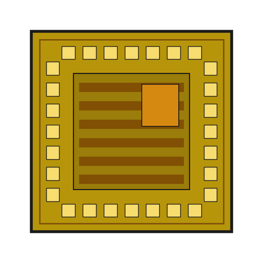
Mẫu thiết kế (template) của wafer.space đi kèm hai macro SRAM trong thiết kế ví dụ, mỗi macro 512 byte, và để chúng ở trạng thái tắt. Macro là một khối bộ nhớ hoàn chỉnh từ PDK: 4.096 ô nhớ tĩnh (static memory cell), được vẽ sẵn một lần cùng với bộ giải mã địa chỉ và mạch đọc, và bạn đặt nguyên khối thay vì phải xây dựng từ các cổng logic. Bậc này bật một trong số đó. Bộ điều chỉnh độ sáng (dimmer) từ bậc trước giờ chạy một chuỗi mẫu: một vi điều khiển ghi 256 byte vào chip qua các chân pad, chỉ một lần, và từ đó chip tự đọc lại chúng, mỗi bước một byte, làm độ sáng của một đèn đang thở chậm rãi. Lõi và testbench của nó được chạy cho bản thiết kế này với Icarus Verilog 12.0, cocotb 2.1.0 và mô hình mô phỏng riêng của PDK dành cho macro SRAM: đầu ra bám theo bảng đã lưu trong 600 chu kỳ PWM. Hình ảnh là đầu ra mô phỏng của chính nó, mỗi thanh một chu kỳ. Bản phác thảo ESP32 nạp bảng này đã được biên dịch cho bản thiết kế này; hiện chưa có chip thật để chạy nó.
Nâng cao
Một buổi tối, cùng với con chip

Hướng dẫn

1

Mẫu, thời điểm và kích thước

Đang tải sổ tay Jupyter…
2

Mỗi trong số 4.096 bit là gì

Sơ đồ thiết kế nhúng cho thấy cách một bit bộ nhớ tĩnh tự giữ trạng thái: một vòng lặp gồm hai bộ đảo (inverter). Khối macro trong bậc này là 4.096 bit bộ nhớ tĩnh trong một mảng duy nhất.
3

Các chân của macro, và ba điều mô hình của nó cho biết

gf180mcu_fd_ip_sram__sram512x8m8wm1 có dung lượng 512 byte. Các chân của nó: CLK; A, địa chỉ 9 bit; D, byte cần ghi; Q, byte được đọc. Ba tín hiệu điều khiển đều tích cực LOW. CEN bằng 0 sẽ bật bộ nhớ. GWEN bằng 0 khiến cạnh xung clock là thao tác ghi, bằng 1 là thao tác đọc. WEN có một bit cho mỗi bit dữ liệu, và khi bằng 0 thì bit đó được phép ghi, nên một thao tác ghi có thể thay đổi một số bit của byte và giữ nguyên các bit còn lại. Đọc mô hình mô phỏng của PDK cho thấy ba điều đáng biết. Thứ nhất, bộ nhớ chỉ hoạt động sau khi CEN chuyển từ 1 xuống 0; nếu không, mô hình in ra "CEN is not reset, memory is not operational", vì vậy lõi giữ CEN ở mức 1 trong suốt quá trình reset và hạ xuống sau đó. Thứ hai, thao tác đọc đưa mem[A] ra Q ngay sau cạnh xung clock lấy mẫu A, nên dữ liệu sẵn sàng sau một chu kỳ clock. Thứ ba, mô hình khởi đầu với mọi byte bằng 0. Chip thực thì không: SRAM của nó khi khởi động mang giá trị ngẫu nhiên mà mỗi ô nhớ rơi vào, nên thiết kế phải ghi trước khi đọc. Ví dụ của template gán CEN bằng 1, nên hai macro của nó bị tắt. Các file timing của nó cho chu kỳ clock tối thiểu của macro là 6,6 ns ở góc điển hình 5 V và 18,3 ns ở góc chậm 3,0 V, 125 °C, cả hai đều nằm trong giới hạn 40 ns của template.
4

The core

src/chip_core.sv for the pattern player, with the template's port list unchanged plus one parameter, HOLD_LOG2. Input pad 0 enables, pad 1 selects LOAD mode, pad 2 is the write strobe; bidirectional pads 0 to 7 carry the byte, pad 8 the PWM. The LOAD and strobe pads are passed through two flip-flops before use, a synchroniser: they change whenever the outside world likes, not in step with the chip's clock, and a flip-flop caught mid-change can hover between 0 and 1 for a while. In play mode, each time HOLD_LOG2 periods have passed, the byte the SRAM has been reading becomes the new duty and the address moves on.
chip_core.svsystemverilog
// SPDX-License-Identifier: Apache-2.0
// Youblob silicon rung 5: the PWM dimmer plays a brightness pattern stored in the on-chip SRAM macro.
// Port list unchanged from wafer-space/gf180mcu-project-template src/chip_core.sv.

`default_nettype none

module chip_core #(
    parameter NUM_INPUT_PADS,
    parameter NUM_BIDIR_PADS,
    parameter NUM_ANALOG_PADS,
    parameter HOLD_LOG2 = 9        // each table entry lasts 2**HOLD_LOG2 PWM periods
    )(
    `ifdef USE_POWER_PINS
    inout  wire VDD,
    inout  wire VSS,
    `endif

    input  wire clk,       // clock
    input  wire rst_n,     // reset (active low)

    input  wire [NUM_INPUT_PADS-1:0] input_in,   // Input value
    output wire [NUM_INPUT_PADS-1:0] input_pu,   // Pull-up
    output wire [NUM_INPUT_PADS-1:0] input_pd,   // Pull-down

    input  wire [NUM_BIDIR_PADS-1:0] bidir_in,   // Input value
    output wire [NUM_BIDIR_PADS-1:0] bidir_out,  // Output value
    output wire [NUM_BIDIR_PADS-1:0] bidir_oe,   // Output enable
    output wire [NUM_BIDIR_PADS-1:0] bidir_cs,   // Input type (0=CMOS Buffer, 1=Schmitt Trigger)
    output wire [NUM_BIDIR_PADS-1:0] bidir_sl,   // Slew rate (0=fast, 1=slow)
    output wire [NUM_BIDIR_PADS-1:0] bidir_ie,   // Input enable
    output wire [NUM_BIDIR_PADS-1:0] bidir_pu,   // Pull-up
    output wire [NUM_BIDIR_PADS-1:0] bidir_pd,   // Pull-down

    inout  wire [NUM_ANALOG_PADS-1:0] analog  // Analog
);

    // Input pad 0: enable.  Input pad 1: LOAD mode.  Input pad 2: write strobe.
    // Bidir pads 0..7: the byte to store while loading.  Bidir pad 8: the PWM output.
    localparam DUTY_W = 8;
    localparam PWM_PAD = 8;

    assign input_pu = '0;
    assign input_pd = '0;
    assign bidir_oe = {{(NUM_BIDIR_PADS-DUTY_W){1'b1}}, {DUTY_W{1'b0}}};
    assign bidir_ie = ~bidir_oe;
    assign bidir_cs = {{(NUM_BIDIR_PADS-DUTY_W){1'b0}}, {DUTY_W{1'b1}}};
    assign bidir_sl = '0;
    assign bidir_pu = '0;
    assign bidir_pd = '0;

    wire enable = input_in[0];
    wire [DUTY_W-1:0] data_in = bidir_in[DUTY_W-1:0];

    // The mode and strobe pads change whenever the outside world likes, not in step with clk:
    // two flip-flops in a row (a synchroniser) before anything uses them.
    logic [1:0] load_s;
    logic [2:0] strobe_s;
    always_ff @(posedge clk) begin
        load_s   <= {load_s[0], input_in[1]};
        strobe_s <= {strobe_s[1:0], input_in[2]};
    end
    logic load_was;
    wire load        = load_s[1];
    wire load_start  = load & ~load_was;
    wire strobe_rise = strobe_s[1] & ~strobe_s[2];
    always_ff @(posedge clk) load_was <= load;

    // The SRAM wants its chip enable (CEN, active LOW) to go 1 -> 0 before it works:
    // hold it at 1 through reset, then 0.
    logic cen;
    always_ff @(posedge clk) cen <= !rst_n;

    // PWM counter and the "hold" counter that decides when to step to the next table entry.
    logic [DUTY_W-1:0] count;
    logic [HOLD_LOG2:0] hold;                   // one bit wider so HOLD_LOG2 = 0 still works
    wire period_end = (count == '1);
    localparam logic [HOLD_LOG2:0] HOLD_MASK = (1 << HOLD_LOG2) - 1;   // 0 when HOLD_LOG2 = 0
    wire step = period_end && ((hold & HOLD_MASK) == HOLD_MASK);

    logic [DUTY_W-1:0] addr;
    logic [DUTY_W-1:0] duty;
    wire  [DUTY_W-1:0] q;                       // SRAM read data: mem[addr], one clock after addr

    always_ff @(posedge clk) begin
        if (!rst_n) begin
            count <= '0;  hold <= '0;  addr <= '0;  duty <= '0;
        end else if (load) begin
            count <= '0;  hold <= '0;  duty <= '0;
            if (load_start)       addr <= '0;       // every load starts at entry 0
            else if (strobe_rise) addr <= addr + 1'b1;
        end else if (enable) begin
            count <= count + 1'b1;
            if (period_end) hold <= hold + 1'b1;
            if (step) begin
                duty <= q;                          // the entry that was being read
                addr <= addr + 1'b1;                // and move on to the next
            end
        end
    end

    `gf180mcu_xxx_ip_sram__sram512x8m8wm1 sram_0 (
        `ifdef USE_POWER_PINS
        .VDD  (VDD),
        .VSS  (VSS),
        `endif
        .CLK  (clk),
        .CEN  (cen),                                   // active low: 0 = on
        .GWEN (~(load && strobe_rise)),                // active low: 0 = write this clock
        .WEN  (8'b0),                                  // active low, per bit: write all eight
        .A    ({1'b0, addr}),                          // 256 of the 512 bytes
        .D    (data_in),
        .Q    (q)
    );

    logic pwm;
    always_ff @(posedge clk) begin
        if (!rst_n) pwm <= 1'b0;
        else        pwm <= enable && !load && (count < duty);
    end

    logic [NUM_BIDIR_PADS-1:0] out;
    always_comb begin
        out = '0;
        out[PWM_PAD] = pwm;
    end
    assign bidir_out = out;

    // Inputs this design does not read (keeps lint quiet, as the template does with _unused).
    logic _unused;
    assign _unused = &{1'b0, input_in[NUM_INPUT_PADS-1:3], bidir_in[NUM_BIDIR_PADS-1:DUTY_W], hold[HOLD_LOG2]};

endmodule

`default_nettype wire

Công cụ cần thiết:

Máy tính để bànMáy tính để bàn
5

The test

test_pattern.py builds the core with the PDK's SRAM model, gf180mcu_fd_ip_sram__sram512x8m8wm1.v, at the template's 25 MHz and with HOLD_LOG2 = 0 so the whole table plays in 256 periods. It loads the table through the pads the way the ESP32 will, then counts the high clocks in each of 600 PWM periods and requires them to follow the table from exactly one starting point. A second test loads again and checks the new pattern replaced the old.
test_pattern.pypython
# SPDX-License-Identifier: Apache-2.0
# cocotb testbench for the SRAM pattern player, with the PDK's own SRAM simulation model
# (gf180mcu_fd_ip_sram__sram512x8m8wm1, gf180mcuD, the commit the template pins).
import math
import os
from pathlib import Path

import cocotb
from cocotb.clock import Clock
from cocotb.triggers import ClockCycles, FallingEdge, RisingEdge
from cocotb_tools.runner import get_runner

PWM_PAD = 8
EN, LOAD, STROBE = 1, 2, 4                      # input pad bits
SRAM = Path(os.getenv("PDK_ROOT", "pdk")) / "gf180mcuD" / "libs.ref" / "gf180mcu_fd_ip_sram" / "verilog"


def breathing_table(n=256, gamma=2.2):
    """One slow breath: a raised sine, gamma-corrected so equal steps LOOK equal to the eye."""
    return [round(255 * ((1 - math.cos(2 * math.pi * i / n)) / 2) ** gamma) for i in range(n)]


async def start(dut):
    cocotb.start_soon(Clock(dut.clk, 40, unit="ns").start())   # 25 MHz, the template's CLOCK_PERIOD
    dut.input_in.value = 0
    dut.bidir_in.value = 0
    dut.rst_n.value = 0
    await ClockCycles(dut.clk, 5)
    dut.rst_n.value = 1
    await ClockCycles(dut.clk, 2)


async def load(dut, table):
    """What a microcontroller on the breakout does: LOAD high, then per byte set the data pads,
    raise the strobe, wait, lower it. The chip synchronises the strobe, so hold each for 4 clocks."""
    dut.input_in.value = LOAD
    await ClockCycles(dut.clk, 4)
    for b in table:
        dut.bidir_in.value = b
        await ClockCycles(dut.clk, 1)
        dut.input_in.value = LOAD | STROBE
        await ClockCycles(dut.clk, 4)
        dut.input_in.value = LOAD
        await ClockCycles(dut.clk, 4)
    dut.input_in.value = 0
    await ClockCycles(dut.clk, 4)


async def highs_per_period(dut, periods):
    """High clocks in each PWM period, counted from the core's own count = 0."""
    while int(dut.count.value) != 0:
        await RisingEdge(dut.clk)
    out = []
    for _ in range(periods):
        n = 0
        for _ in range(256):
            await FallingEdge(dut.clk)
            n += int(dut.bidir_out.value[PWM_PAD])
        out.append(n)
    return out


@cocotb.test()
async def test_plays_the_table(dut):
    """Load a 256-entry breathing table, play it: each period's high time is the next entry."""
    table = breathing_table()
    await start(dut)
    await load(dut, table)
    dut.input_in.value = EN
    got = await highs_per_period(dut, 600)
    # the output starts part-way through the table; find where, then demand every period match
    fits = [off for off in range(256) if all(got[j] == table[(j + off) % 256] for j in range(2, 600))]
    dut._log.info(f"first periods {got[:8]}, table aligns at offset {fits}")
    Path(__file__).resolve().parent.joinpath("pattern_trace.csv").write_text("\n".join(map(str, got)))
    assert len(fits) == 1, f"the output does not follow the table (offsets that fit: {fits})"


@cocotb.test()
async def test_reload(dut):
    """Loading again replaces the pattern: a flat 64 gives 64 high clocks every period."""
    await start(dut)
    await load(dut, breathing_table())
    await load(dut, [64] * 256)
    dut.input_in.value = EN
    got = await highs_per_period(dut, 40)
    assert all(g == 64 for g in got[2:]), got


def test_runner():
    here = Path(__file__).resolve().parent
    defines = {"gf180mcu_xxx_ip_sram__sram512x8m8wm1": "gf180mcu_fd_ip_sram__sram512x8m8wm1"}
    runner = get_runner("icarus")
    runner.build(
        sources=[SRAM / "gf180mcu_fd_ip_sram__sram512x8m8wm1.v", here / "chip_core.sv"],
        hdl_toplevel="chip_core",
        parameters={"NUM_INPUT_PADS": 4, "NUM_BIDIR_PADS": 38, "NUM_ANALOG_PADS": 4, "HOLD_LOG2": 0},
        defines=defines,
        build_args=["-g2012"],
        timescale=("1ns", "1ps"),
        always=True,
    )
    runner.test(hdl_toplevel="chip_core", test_module="test_pattern")


if __name__ == "__main__":
    test_runner()

Công cụ cần thiết:

Máy tính để bànMáy tính để bàn
6

Những gì mô phỏng đã in ra

Chạy cho blueprint này với Icarus Verilog 12.0 và cocotb 2.1.0: -------- MESSAGE: CEN vừa được reset, bộ nhớ hoạt động --------- test_pattern.test_plays_the_table PASS (600 chu kỳ, bảng khớp chính xác tại một offset) test_pattern.test_reload PASS TESTS=2 PASS=2 FAIL=0 SKIP=0 Để chứng minh test có thể thất bại, WEN đã được đổi từ 8'b0 thành 8'hFF, lỗi kinh điển với chân active-low: mọi bit bị che, không có gì được ghi, và bảng toàn số không. Cả hai test đều thất bại, và core đã được khôi phục. Dòng đầu tiên là thông báo riêng của mô hình SRAM: core đã kéo CEN xuống thấp sau reset, như mô hình yêu cầu.
7

Load it from an ESP32

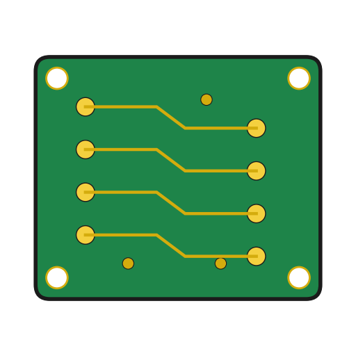
Once the chip is on its breakout board, this sketch writes the table. Eight GPIOs carry the byte, three more drive LOAD, the strobe and enable, and an LED with a 330 ohm resistor from pad 8 to ground shows the breath. Each level is held for 1 microsecond, 25 of the chip's clocks, so the synchroniser always sees it. The sketch then does nothing: the pattern lives in the chip. It is lost when the chip loses power, so send r over serial to load it again. The ESP32 is a 3.3 V part and its inputs are not 5 V tolerant. The sketch only drives the chip and never reads from it. The template's default libraries are the 5 V ones; before you connect, check in the I/O library's documentation that 3.3 V is a valid logic high for your chip's inputs, or build with the 3.3 V libraries, as the template's README shows. The sketch compiles for the ESP32 with the Arduino ESP32 core 3.3.12; it has not been run, because the chip does not exist yet.
load_pattern.inocpp
// SPDX-License-Identifier: Apache-2.0
// Load a breathing pattern into your chip's SRAM through its pads, then let the chip play it.
// Youblob silicon rung 5. The chip does the playing; this board only writes 256 bytes once.
//
// Wiring (ESP32 GPIO -> chip pad on your breakout):
//   D0..D7  GPIO 13,14,18,19,21,22,23,25 -> bidir[0..7]
//   LOAD    GPIO 26 -> input[1]
//   STROBE  GPIO 27 -> input[2]
//   EN      GPIO 32 -> input[0]
//   and a common ground. The chip's bidir[8] drives an LED through 330 ohm to ground.
// The ESP32 is a 3.3 V part: run the chip's I/O at 3.3 V, or put a level shifter between them.

#include <math.h>

const int DATA_PINS[8] = {13, 14, 18, 19, 21, 22, 23, 25};
const int PIN_LOAD = 26, PIN_STROBE = 27, PIN_EN = 32;

// The chip passes LOAD and STROBE through a two-flip-flop synchroniser and looks for the strobe's
// rising edge, so every level has to last a few of ITS clocks. 1 us is 25 clocks at 25 MHz.
const unsigned HOLD_US = 1;

uint8_t table[256];

void makeBreathingTable() {
  // a raised sine, gamma-corrected (2.2) so the brightness steps look even to the eye
  for (int i = 0; i < 256; i++) {
    float s = (1.0f - cosf(2.0f * PI * i / 256.0f)) / 2.0f;
    table[i] = (uint8_t)lroundf(255.0f * powf(s, 2.2f));
  }
}

void putByte(uint8_t b) {
  for (int bit = 0; bit < 8; bit++) digitalWrite(DATA_PINS[bit], (b >> bit) & 1);
  delayMicroseconds(HOLD_US);            // data settles before the strobe
  digitalWrite(PIN_STROBE, HIGH);        // the chip writes on the strobe's rising edge...
  delayMicroseconds(HOLD_US);            // ...a few of its clocks later, so hold the data
  digitalWrite(PIN_STROBE, LOW);
  delayMicroseconds(HOLD_US);
}

void loadTable() {
  digitalWrite(PIN_EN, LOW);
  digitalWrite(PIN_LOAD, HIGH);          // entering LOAD resets the chip's address to 0
  delayMicroseconds(HOLD_US);
  for (int i = 0; i < 256; i++) putByte(table[i]);
  digitalWrite(PIN_LOAD, LOW);
  delayMicroseconds(HOLD_US);
}

void setup() {
  Serial.begin(115200);
  for (int bit = 0; bit < 8; bit++) pinMode(DATA_PINS[bit], OUTPUT);
  pinMode(PIN_LOAD, OUTPUT);
  pinMode(PIN_STROBE, OUTPUT);
  pinMode(PIN_EN, OUTPUT);
  digitalWrite(PIN_STROBE, LOW);

  makeBreathingTable();
  loadTable();
  digitalWrite(PIN_EN, HIGH);            // play
  Serial.println("pattern loaded; the chip is playing it on its own");
  Serial.printf("table[0]=%u table[64]=%u table[128]=%u\n", table[0], table[64], table[128]);
}

void loop() {
  // Nothing to do: the pattern lives in the chip's SRAM now.
  // Send 'r' over serial to load it again (the SRAM loses it when the chip loses power).
  if (Serial.available() && Serial.read() == 'r') {
    loadTable();
    digitalWrite(PIN_EN, HIGH);
    Serial.println("reloaded");
  }
}

Vật liệu cho bước này:

Chip ASIC tùy chỉnhChip ASIC tùy chỉnh1 cái
Bảng mạch inBảng mạch in1 cái
LED 5 mmLED 5 mm1 cái
Điện trở 330 ohmĐiện trở 330 ohm1 cái

Công cụ cần thiết:

Bo mạch phát triển ESP32Bo mạch phát triển ESP32
Bảng cắm mạchBảng cắm mạch
Dây nốiDây nối
Máy tính để bànMáy tính để bàn
8

Mẫu không lưu được hoặc không phát được

Khắc phục sự cố mẫu SRAM.

Flow

Loading...
9

Nguồn và giới hạn trung thực

**Nguồn**, đọc ngày 29 tháng 9 năm 2026: GF180MCU PDK tại commit mà template ghim (gf180mcuD, f6eeac7dad085ffcc829ccfd721f7b4ce39edcf7, từ các bản phát hành fossi-foundation ciel; Apache-2.0): mô hình SRAM gf180mcu_fd_ip_sram__sram512x8m8wm1.v, LEF của nó cho đường viền và các tệp thời gian của nó cho chu kỳ xung nhỏ nhất; tệp thời gian của thư viện standard-cell cho diện tích flip-flop. Kho wafer-space/gf180mcu-project-template (src/chip_core.sv, src/chip_top.sv, README.md, librelane/config.yaml; Apache-2.0). **Giới hạn trung thực.** Mô phỏng ở mức chip_core, với mô hình riêng của SRAM nhưng không có vành pad, tổng hợp hay layout, và các kiểm tra thời gian của mô hình không quyết định điều gì ở đây. Bản phác thảo ESP32 đã được biên dịch, chưa được chạy. HOLD_LOG2 bằng 0 trong bài kiểm tra để nó kết thúc; chip sẽ dùng 9, một nhịp thở khoảng 1,3 s.

Vật liệu

4

Công cụ yêu cầu

4

CC0 Phạm vi công cộng

Bản thiết kế này được phát hành theo CC0. Bạn tự do sao chép, sửa đổi, phân phối và sử dụng cho bất kỳ mục đích nào mà không cần xin phép.

Hỗ trợ nhà sáng tạo bằng cách mua sản phẩm qua bản thiết kế, nơi họ nhận Hoa hồng nhà sáng tạo do nhà bán hàng đặt, hoặc tạo phiên bản mới và kết nối trong bản thiết kế riêng để chia sẻ doanh thu.

Thảo luận

(0)

Đăng nhập để tham gia thảo luận

Đang tải bình luận...