NGHỆ THUẬT
LÀM ĐẸP VÀ SỨC KHỎE
THỦ CÔNG
VĂN HÓA VÀ LỊCH SỬ
GIẢI TRÍ
MÔI TRƯỜNG
THỰC PHẨM VÀ ĐỒ UỐNG
KỸ THUẬT NGƯỢC
KHOA HỌC
THỂ THAO
CÔNG NGHỆ
THIẾT BỊ ĐEO

The Chip-on-Board Breakout: From a 0.4 mm Mezzanine to Pins You Can Reach
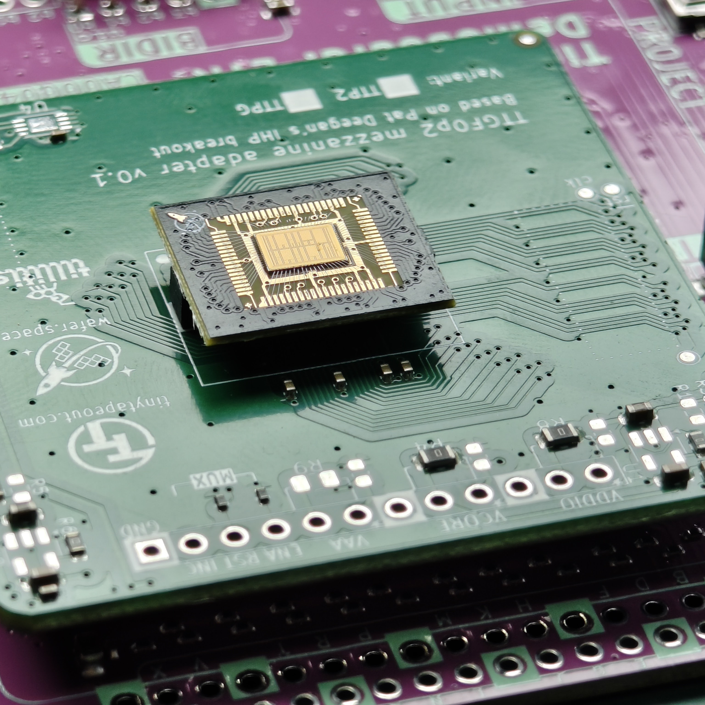
A chip from a shared wafer comes back tiny. On wafer.space's Run 1 it arrived as a chip-on-board part 14 × 16 mm, with the die wire-bonded under epoxy and a 70-pin mezzanine connector underneath at 0.4 mm pitch. Nothing on a bench can touch pins that small, so the first thing to build is a board that carries them back out.
wafer.space publishes example breakout motherboards in KiCad under Apache-2.0: one sheet, two boards. Each has the mating 70-pin mezzanine socket; one breaks the pins out to two 1 × 35 rows of 0.1-inch pin headers, the other to two rows of 35 castellated edge pads at 1 mm.
This rung works out why the fine pitch is needed and what spreading it out costs in board length, shows the published schematic, and builds the header version.
Nâng cao
About a day of soldering, plus board fabrication
Hướng dẫn
1
1
Pitch against board edge
Pitch against board edge
Đang tải sổ tay Jupyter…
2
2
Where the chip comes from
Where the chip comes from
The embedded blueprint designs the chip and orders it. This rung builds the board it plugs into.
3
3
What the chip-on-board plugs into
What the chip-on-board plugs into
From wafer.space's Run 1 documentation: the full-slot chip-on-board is 14 × 16 mm; the die's 74 bond pads follow the Tiny Tapeout convention, and all grounds are tied together on the default breakout. It carries a 70-pin, 0.4 mm pitch mezzanine connector (LCSC C19089236; the mating part is LCSC C19089262).
So that every project fits the same boards, the default breakouts share the same wire-bonding layout, the same 14 × 16 mm footprint and the same connector position; traces, signal types and net assignments are left to the designer. wafer.space notes that pinouts, connectors and footprints are specific to each run.
4
4
The published breakout schematic
The published breakout schematic
wafer.space's example motherboards, from the chip-on-board-wire-bonded-pcbs repository (run-1/motherboards, Apache-2.0), shown as published. On the left, the ".1\" Header" board: the mezzanine socket J102 (HCTL HC-PBB40C-70DP-0.4V-02, 70 pins at 0.4 mm) broken out to the 1 × 35 pin headers J101 and J103 at 2.54 mm. On the right, the "Castellated" board: the same socket J105 broken out to the 1 × 35 castellated edges J104 and J106 at 1 mm, so the whole breakout can itself be soldered onto a larger board.
Đang tải trình xem KiCanvas...
Trình xem thiết kế PCB chuyên nghiệp
5
5
Build the header board
Build the header board
Download the run-1/motherboards project from the repository and open it in KiCad. The files are saved by KiCad 10, so an older KiCad will not open them. Plot the Gerber and drill files and order the board from a PCB fabricator, with a solder-paste stencil for the mezzanine footprint.
Hold the stencil over the mezzanine pads and spread lead-free solder paste across it in one stroke. Place the socket with fine tweezers, square to its pads, and reflow it with the hot-air station until the paste flows and settles. Inspect every one of the 70 joints with the loupe; clear any bridge between neighbouring pins with flux and the iron or hot air.
Solder the two 1 × 35 pin headers with the iron. Before you plug in a chip, check with the multimeter that no two neighbouring header pins are shorted, and that each header pin reaches the socket pin the schematic connects it to.
Vật liệu cho bước này:
 Bảng mạch in1 cái
 Đầu nối bo mạch với bo mạch1 cái
 Hàng chân cắm2 cái
 Kem hàn (không chì)1 cái
 Thiếc hàn chì1 cái
 Chất trợ chảy1 cái
Công cụ cần thiết:
 Trạm khò khí nóng
 Mỏ hàn
 Nhíp đầu nhọn
 Kính lúp thợ kim hoàn
 Đồng hồ vạn năng
 Máy tính để bàn
6
6
A breakout that shorts or does not connect
A breakout that shorts or does not connect
Breakout board troubleshooting.
Flow
Loading...
7
7
Sources and honest limits
Sources and honest limits
**Sources**, read 29 September 2026: wafer.space's chip-on-board-wire-bonded-pcbs repository (README, run-1/README and run-1/motherboards, Apache-2.0). The schematic in step 4 is theirs, unchanged. The photograph is theirs too, from the same repository: a Run 1 chip-on-board seated on a Tiny Tapeout mezzanine adapter board (TTGF02, v0.1), not the header board built in step 5.
**Honest limits.** This rung has not been built for this blueprint; the soldering steps are standard practice for a 0.4 mm surface-mount connector, not wafer.space instructions. The pinout and footprint are Run 1's, and wafer.space says they are expected to change in later runs, so check the current run's documentation before ordering boards.
Vật liệu
6- 1 cáiTạm thời
- Tạm thời
- từ$1.17
- 1 cáiTạm thời
- 1 cáiTạm thời
- 1 cáiTạm thời
Công cụ yêu cầu
6- Tạm thời
- Tạm thời
- Tạm thời
- Tạm thời
- Tạm thời
Blueprint liên quan
Các blueprint này chia sẻ kiến thức — kỹ thuật, vật liệu hoặc nguyên tắc


CC0 Phạm vi công cộng
Bản thiết kế này được phát hành theo CC0. Bạn tự do sao chép, sửa đổi, phân phối và sử dụng cho bất kỳ mục đích nào mà không cần xin phép.
Hỗ trợ nhà sáng tạo bằng cách mua sản phẩm qua bản thiết kế, nơi họ nhận Hoa hồng nhà sáng tạo do nhà bán hàng đặt, hoặc tạo phiên bản mới và kết nối trong bản thiết kế riêng để chia sẻ doanh thu.